
Product Specifications
Frequency Range: 35MHz to 4.4GHz
Output level range: -60dBm~0dBm
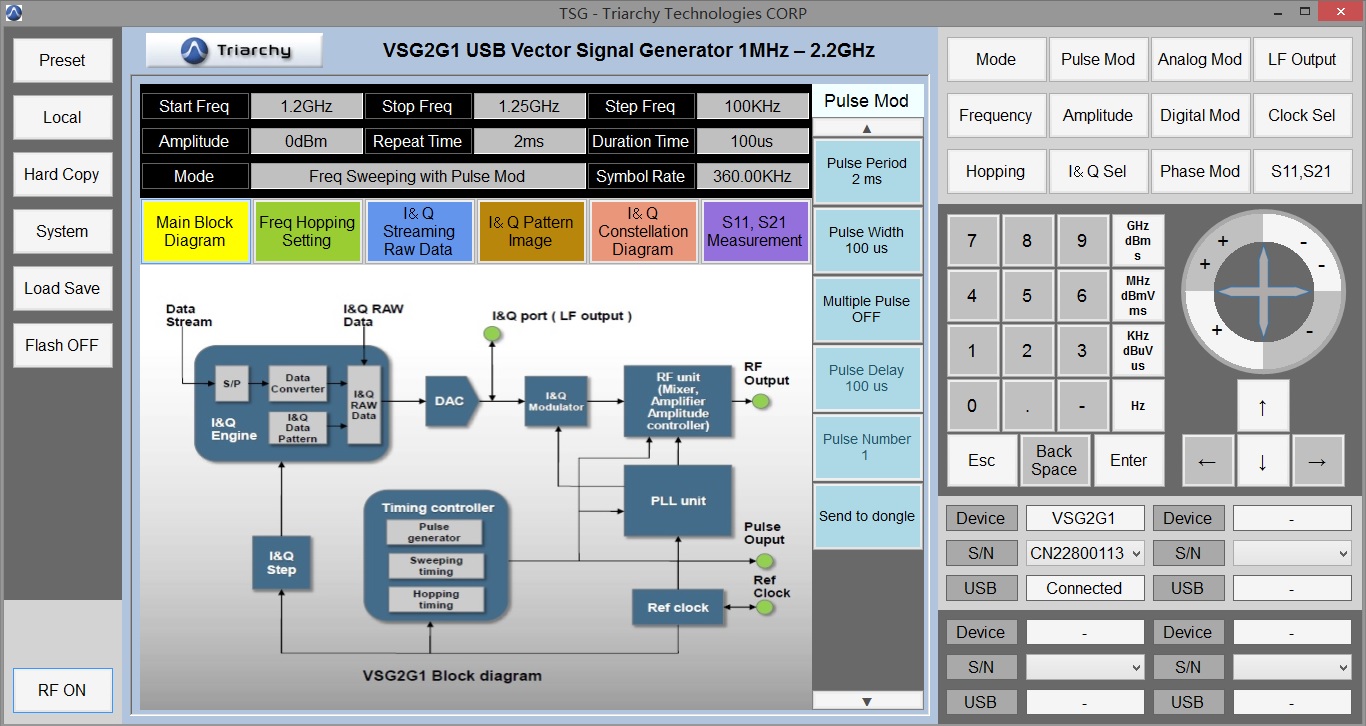
Working mode: CW mode, frequency sweeping, frequency hopping, pulse modulation and simutaneous I&Q modulation
LF signal generator: Sin, triangle waveform, arbitrary signal waveform
Pulse signal generator
Product Features
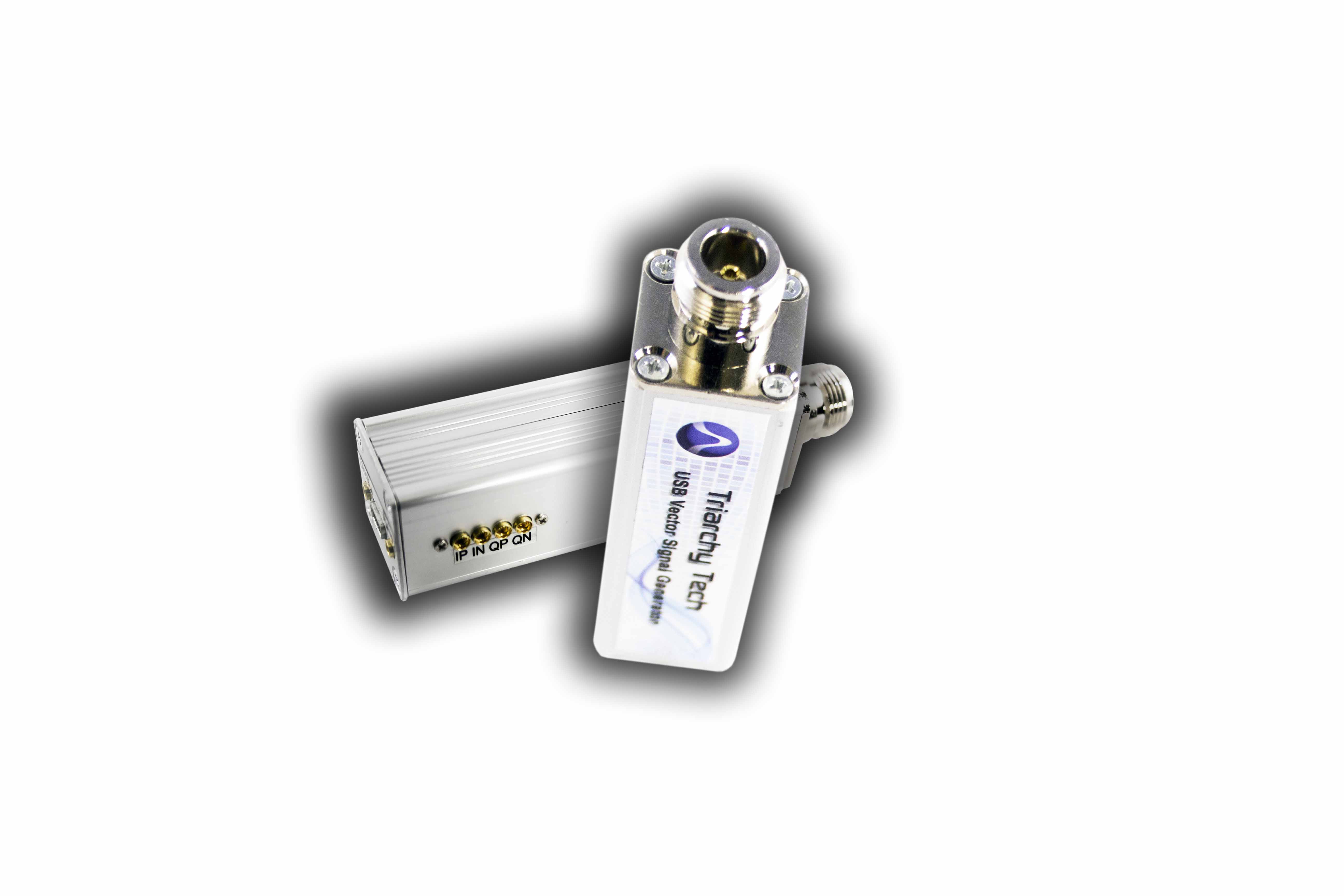
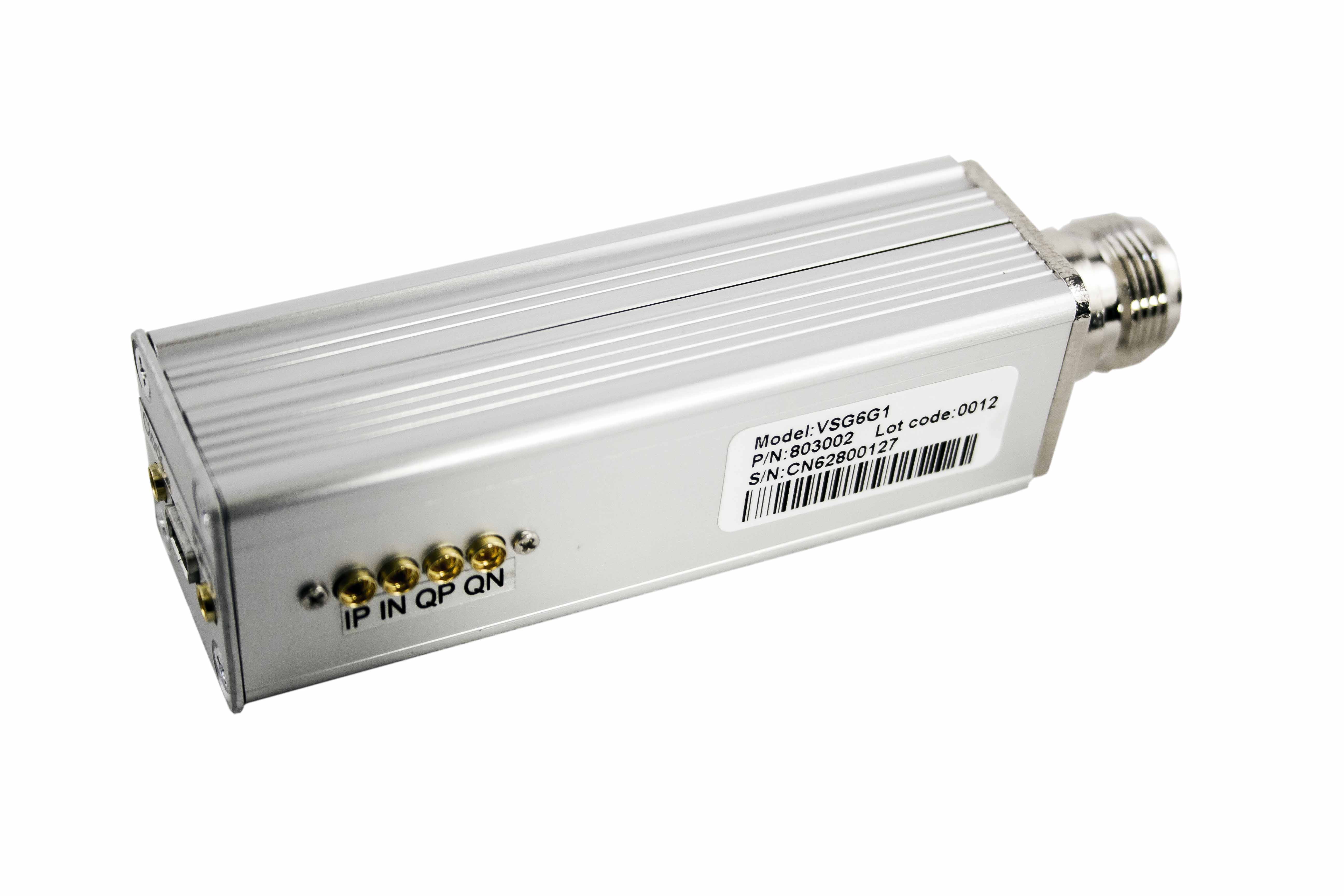
Probe size USB device, with N connector and solid metal case
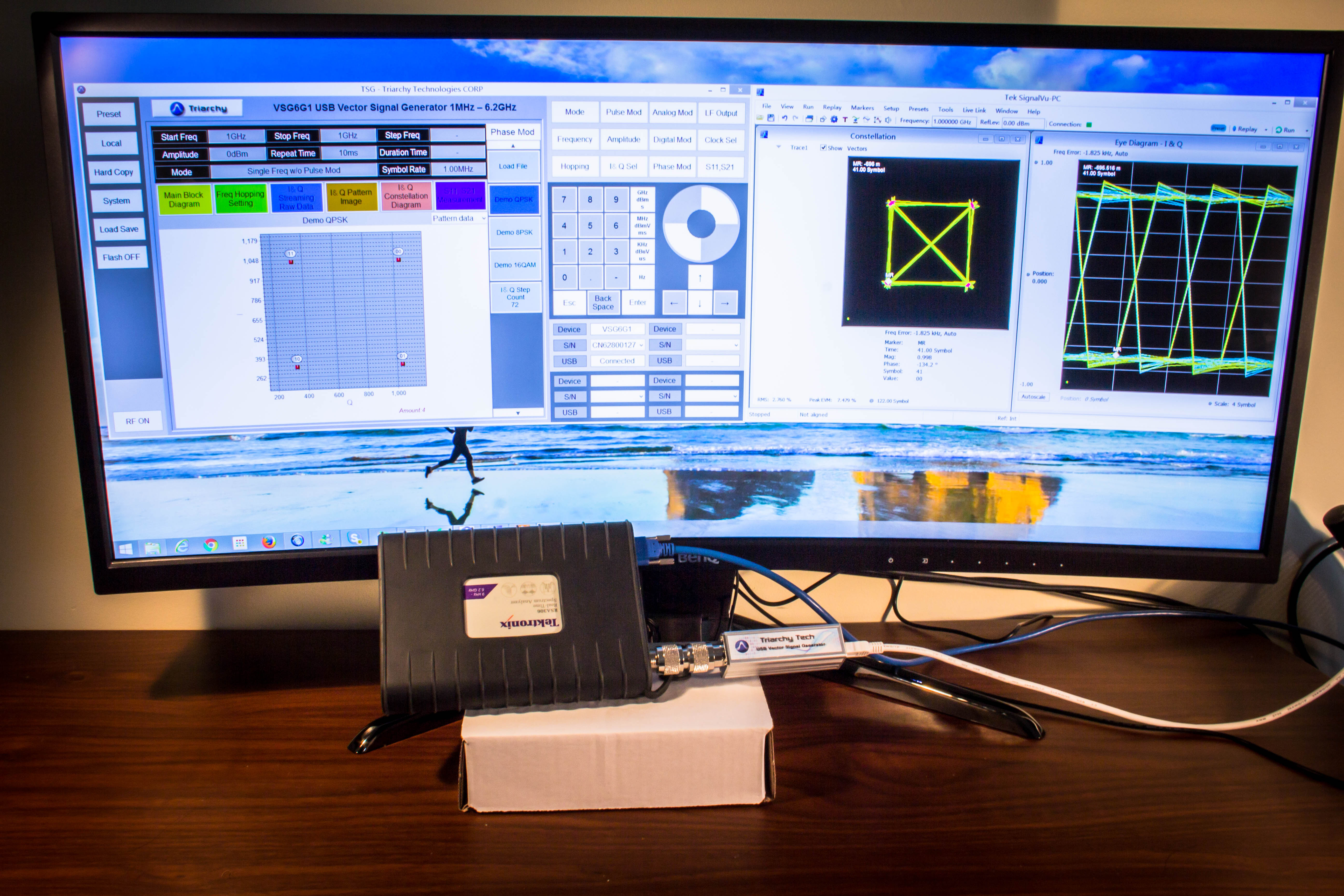
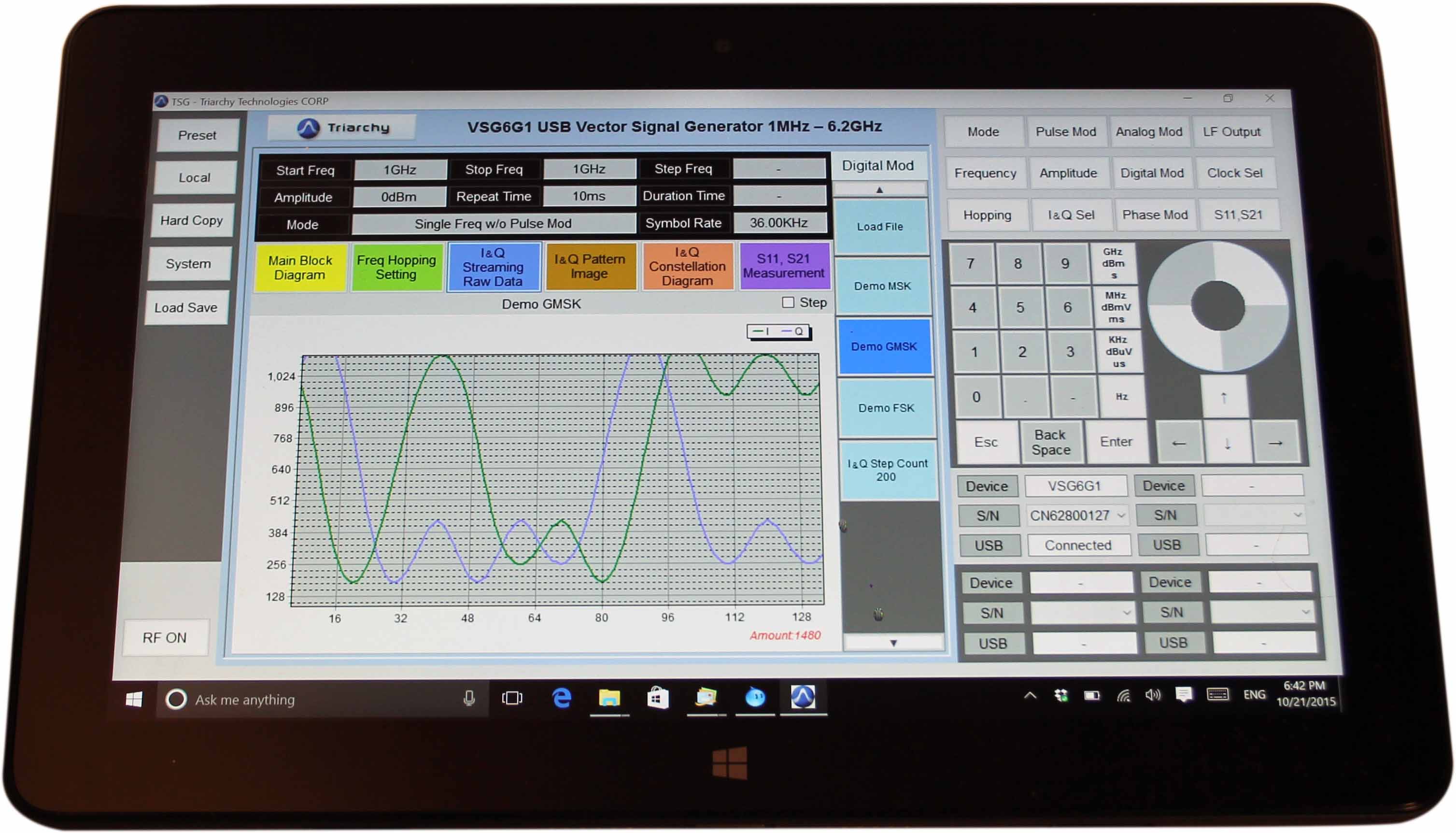
Intuitive PC program GUI inspired by desktop instrument front panel
Built-in arbitrary function generator to generator LF signal output
Pulse output at rear panel working as Pulse generator
Extra Low cost, extra low weight, best performance for price
Reference clock input and output
USB power without extra battery pack
Standalone working with only 5V power
Product Details
Price: $349 USD
Shipping Cost: $10 CAN/US, $30 International
Shipping Method: USPS First Class Package or Canada Post Tracket Packet (2 - 5 business days). Please contact us if you require expediated shipping. Weekend shipping might be arranged.
Handling Time: >3 business days
Shipping Weight: 9 oz
Dimensions: 100mm x 25mm x 25mm (L x W x H)
VSG2G1/TSG4G1/VSG6G1 Model Selection Guide
Choosing the TSG4G1
The TSG4G1 is suited to applications that don't need I&Q channel for generating
modulation signals, and the frequency requirement is lower than 4.4GHz.
The TSG4G1's signal output is from an ADF4351, with the output level calibrated and
controlled.
The TSG4G1 can also work uncalibrated with a large output level (up to 16dBm at some
frequency points).
Spurious signals are less when the output frequency is between 700MHz and 4400MHz,
so the TSG4G1 can work with a power meter to test S11 andS21 at this band.
The TSG4G1 works with pulse modulation, frequency sweeping and hopping.
The TSG4G1 also have an LF signal output and a pulse signal output for lower frequency
applications.
Limitation with the TSG4G1
When the frequency is lower than 700MHz, more spurious signals will be apparent due to
the ADF4351's RF divider. A divider design cannot be used to achieve problem-free low
frequencies, and other solutions are too costly for the targeted price point. Any RF signal
generator using a ADF4351/ADF4355/RFMD2081 combination will have this problem.
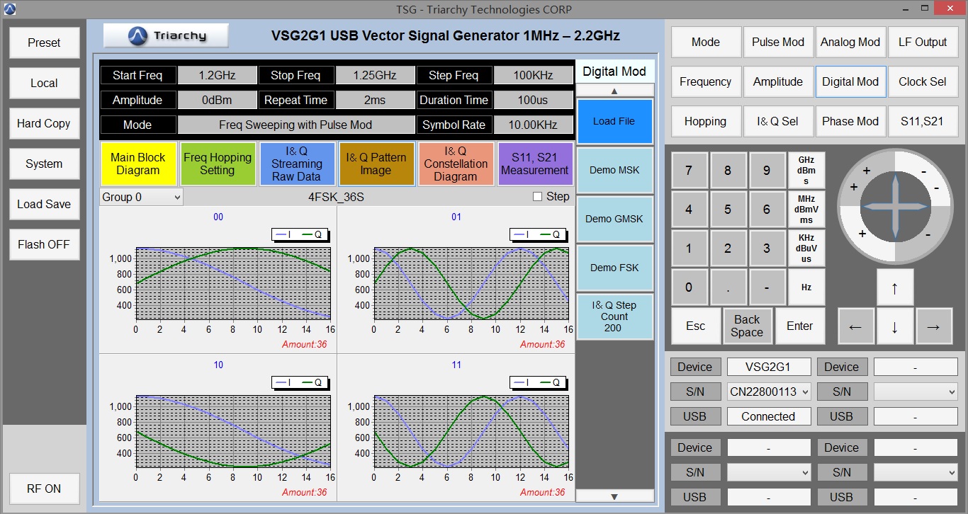
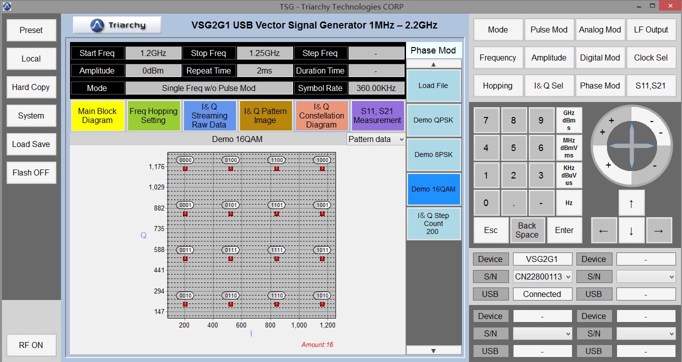
Choosing the VSG2G1
The VSG2G1 is suited to applications that need I&Q channels to generate modulation
signals for testing an RF receiver with frequency requirements lower than 2.2GHz.
The VSG2G1 signal output is from an ADL5385 with the output level calibrated and
controlled.
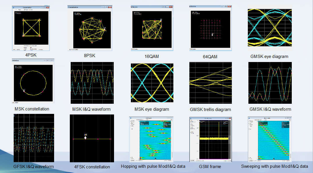
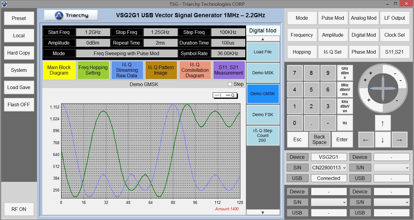
With I&Q modulation provided, the output signal is very useful for most communication
systems. The VSG2G1 can generate signals from simple modulation types (e.g. FM) to
more complex modulations (e.g. QAM)
The I&Q engine in the TSG program provided can easily generate most common
communication signals. Customers can use the program to build custom modulations as
needed. The VSG2G1 can be used for many applications, ranging from radio to cellular
phone testing, for instance.
The ADL5385's bandwidth can extend to 500MHz. While the internal I&Q signal clock is
only effective up to 2.4MHz, an external input works up to 500MHz bandwidth. High speed
I&Q option will work with this interface to generate wide band modulation signals.
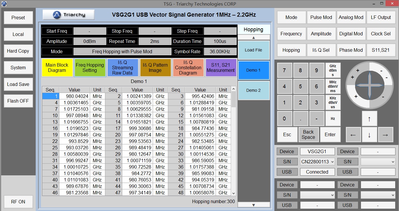
The VSG2G1 can work with pulse modulation, frequency sweeping and hopping to
generate various system signals such TDMA, CDMA, etc.
The VSG2G1 also has both an LF signal output and a pulse signal output for lower
frequency applications.
Limitation with the VSG2G1
The VSG2G1 signal output is from an ADL5385, and the LO source is an ADF4351. It has
same issue as the TSG4G1: the lower the frequency, increasing spurii will be naturally
generated due to the RF divider.
A solution for a modulator with ADL5385 +ADF4351 or using a single chip modulator
RFMD2081 (PLL+ modulator) will have same issue because of the use of a PLL divider for
generating low frequencies. The system design is simple to implement but a trade-off
between the cost and performance.
The harmonics cannot be easily removed, because cost limitations prevent the
implementation of an RF tracking filter.
If the VSG2G1 is used for testing radio receivers, then most receivers will feature a filter
both at the front-end and at the internal IF section anyway, so spurious signals may not be a
serious problem.
Choosing the VSG6G1
The VSG6G1 is ideal if your application needs I&Q channels to generate modulation
signals for testing RF receivers, or the maximum output frequency is needed up to 6.2GHz.
The VSG6G1 signal outputs are a combination of the VSG2G1 and the 2~6GHz section.
The 2~6G section output comes from mixing the VSG2G1 output and the TSG4G1 output
so that the 2~6G section looks like a tripler of the VSG2G1 signal.
The VSG6G1 output is exactly same as the VSG2G1 from 1MHz~2.2GHz. Higher than
2.2GHz, the I&Q channels will only work based on frequency modulation. Please see the
limitation section for details.
The ADL5385's bandwidth can work up to 500MHz. While the internal I&Q signal clock
range is only up to 2.4MHz, the external interface works up to 500MHz bandwidth. A high
speed I&Q option will work with this interface to generate a wide band modulation signal.
The VSG6G1 can work with pulse modulation, frequency sweeping and hopping to
generate many different system signals such TDMA, CDMA, etc.
The VSG6G1 also has an LF signal output and pulse signal output for lower frequency
applications.
Limitation with the VSG6G1
The VSG6G1 covers the VSG2G1 range, so that VSG2G1 issues will be the same on the
VSG6G1. The lower the frequency, the more spurious signals will be generated due to the
RF divider design.
The 2~6G section works as a signal tripler, so more spurious signals will occur in the 2~6G
section. For example, if the output frequency is 6GHz, sub-harmonic 2GHz and 4GHz
spurious signals will appear - sometimes at higher levels.
Also due to the Tripler design, phase distortion can occur in the 2~6G section. Phase
modulation such as PSK, QAM, is not suited for working with the 2~6G section, since
additional modulation is derived from the frequency shift. Signals insensitive to phase
distortion, such as FSK/GFSK, are examples of the kind of modulations are ok.
Product Links
TSG4G1 Software Download (v1.0 .rar)
TSG4G1 User Manual (v1.0 PDF)
TSG4G1 Data Sheet (v1.0 PDF)
TSG4G1 API download page
triarchytech.com download page for application notes and data sheet for other TSA series
For product inquiry: info@triarchytech.com
For product support: support@triarchytech.com
*If your location is on the exclusion list, please contact us via info@triarchytech.com for ordering inquiries.
 Product Image Gallery
 Other Triarchy Products
 USB Vector Signal Generator VSG2G1 1MHz - 2.2GHz | $399USD
Product Page | eBay Page
USB Syntheszied Signal Generator TSG4G1 35MHz - 4.4GHz | $349USD
Product Page | eBay Page
USB Vector Signal Generator VSG6G1 1MHz - 4.2GHz | $449USD
Product Page | eBay Page
 USB Mini Spectrum Analyzer TSA4G1 1MHz - 4.15GHz | $529USD
Product Page | eBay Page
USB Mini Spectrum Analyzer TSA6G1 1MHz - 6.15GHz | $629USD
Product Page | eBay Page
USB Mini Spectrum Analyzer TSA8G1 1MHz - 8.15GHz | $699USD
Product Page | eBay Page
USB Mini Spectrum Analyzer TSA12G5 4GHz - 13.5GHz | $999USD
Product Page | eBay Page
 TNP6Gx Near-Field Probe 4 Piece Set | $99USD
Used with TSA series USB Mini Spectrum Analyzer for EMC pre-testing for CE, FCC or other standards
Product Page | EMC pre-test guide (.PDF)
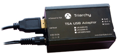 TSA USB Adaptor USB2RS232
Product Page
TSA USB Adaptor USB2WIFI
Product Page
TSA USB Adaptor USB2RJ45
Product Page
Back to Top