Tech highlights
All-discrete fully-complementary topology, Complete symmetry from input to output.
JFET + BJT+ MOSFET
Three types of transistors used to best exploit their strengths.
Pure class A operation,Every stage operates in class A.
Dynamic cascoding,Every stage is dynamically cascoded.
Moderate global negative feedback.
High speed, wide bandwidth.
Fully direct-coupled,There are no signal-degrading coupling capacitors at the input, output or negative feedback loop.
High PSRR design,The power rails are connected
directly to the output stage MOSFETs.
High power output.
Adjustable bias and output DC offset.
Passive ground, active ground or fully balanced configurations.
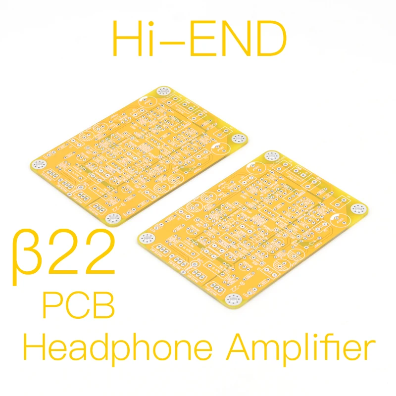
PCB SIZE: 99x70x1.6mm 1oz Cu, HASL with lead
Power requirements: Best:±30VDC I=1A
Schematic & key point of debugging
PCB comes with component parameters for easy installation.
We only refer the schematic of the amplification part of the circuit. If you need full circuit parameter, please read the component value with the PCB by yourself; we do not provide additionally.
please keep test point voltage close enough to it, +-20% is also permitted.


Parts list

Instructions
Since the PCB holes are plated through, you only need to solder the parts from the bottom of the board. Do not drill or enlarge the holes because that would damage the through-plating.
Clean both sides of the blank PCB with paper towel and isopropyl alcohol or electronics flux remover, then solder the components to the board, starting with the lowest profile parts.
Make sure the correct part goes into each position on the circuit board. Measure each resistor with your multimeter to ensure it's the proper value.
Clean up the solder flux residue from the board with isopropyl alcohol (or electronics flux remover) and a brush.
Inspect all solder connections carefully, using a magnifying glass, to make sure there are no solder bridges or cold solder joints. Use a multimeter in ohms scale to check for short circuits. As a minimum, you should verify that the V+ and V- DC inputs are not shorted to ground, or to each other, and that the output pad isn't shorted to ground. Correct any mistakes before proceeding to the next phase.
Tips:
please prepare external heatsink.
Adjust 200R-VR clockwise to the maximum resistance value before powering on.
Adjust 500R-VR counter clockwise to the maximum resistance value before powering on.
After power-on, slowly adjust 200R-VR counterclockwise until 4.4VDC can be measured betweenA
slowly adjust 500R-VR clockwise until 56mVDC can be measured between BC.BD.
Adjiuest 5K-VR,to make <10mV Between both ends of B-O.
Pics
Shippment:
1.We provide free shipping to international via China Post Airmail or Hong Kong Post Airmail, and every parcel will be registered with tracking number. We can also ship by UPS/EMS/DHL/FedEx for alternative shipping method for corresponding fees. Please let us know before payment if you need split shipment.
2.International shipping requires complicated shipping procedures (such as both countries customs, transit stations etc.), also will be affected by many factors, such as holidays, weather conditions etc, If you have not received your shipment within 30 days from payment, please contact us.
3.Time of Delivery:Based on the China Post Airmail or Hong Kong Post Airmail and our experience, kindly please be noted that To United States / United Kingdom / Australia, it takes around 10-15 business days; To Canada, it takes around 12-18 business days; To Brazil / South America, it takes around 25-35 business days. To Italy / France / Spain / Germany/ Eastern Europe, it takes aournd 15-20 business days.
Returns & Replacements & Repair:
We accept returns & replacements within 30 days from the day the customer receive the products, please make first contact within 30 days from receiving the order. Products should be returned in original condition. As a benefit to our customers, we also provide repair within 3 months from the day when this item is shipped out, after repair is done, we will send you the item, but the customer should pay both shipping ways.
Feedback:
1)Your Feedback is really important to us, please take a few seconds to leave great feedback if you are satisfied with our product or service, thank you so much!
2)We always offer the lowest price for best goods and service to you.
3) Please contact us before leaving neutral(3 stars) or negative(1-2 stars) feedback.We will try our best to solve the problem and leave you a happy shopping mood here. Thank you!
