Low Noise R-core transformer DC LPS / Linear Power Supply
Input voltage: AC 115V or 230V (for choose)
Output voltage: DC12V
Continuous current 6A
Front panel: Black ( can provide silver)
display color: blue ( can provide Red or Green)
power switch LED color: blue (can provide Red or Green)
Dimensions: 210mm Width X 70mm high X 257mm deep
Transformer : 100VA OFC R-core transformer
Weight: about 4.5kg
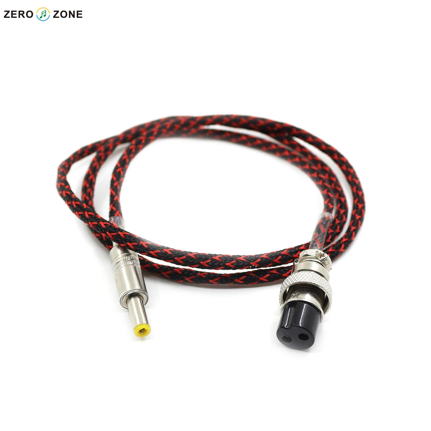
DC Head Size: Outer diameter 5.5mm, internal diameter 2.1mm ( if you need other Size DC head, Please contact us)
Power Polarity: inner"+" external"-"
Package include: Finished linear Power supply X 1
1.2M Teflon silver wire output DC cable X 1 (5.5*2.1mm)
Default is not include the AC input cable.
---------------------------------------------------------------------------------------------------------------------------------------------------------------------------
we have following several kinds voltage for choose.
Output voltage / current
1、5V@6A
2、9V@6A
3、12V@6A
4、15V@5.3A
5、18V@4.4A
6、19V@4.2A
7、24V@3.3A
if you need other voltage, we can accept custom-make.
------------------------------------------------------------------------------------------------------------------------------------
Technical highlights
All-discrete topology.
Single-pass, series regulator design.
No
IC (integrated circuits) are used. This allows complete design control
over all operating points and parameters for superior performance.
Low noise, high PSRR
A
constant-current source feeds a zener diode as a stable voltage
reference. A low-pass filter (with a corner frequency of 1.6Hz) prevents
zener noise from being introduced into the error amplifier. This is an
effective yet lower-cost alternative to expensive voltage reference ICs.
The low-pass filter also provides a soft-start characteristic.
The
output noise (unloaded) is less than 13µV at 24VDC output (measured
using a Tangent LNMP (low-noise measurement preamplifier) and a Fluke
187 50000-count DMM in ACmV mode). The output noise is even less when
the output voltage is lower. This is much better than the noise of an IC
regulator based PSU tested under identical conditions.
The error
amplifier is a discrete implementation of an opamp with a high open-loop
gain of 102.5dB. The voltage supply to the error amplifier is isolated
with capacitance multipliers to boost its PSRR (power supply rejection
ratio). This greatly improves the line regulation performance of the
PSU.
A long-tailed pair differential amplifier with current mirror
and constant current source forms the first stage of the error
amplifier. The second stage is the voltage amplification stage (VAS),
also with constant current source load. The 3rd stage is comprised of
the power MOSFET output devices configured as a source follower.
Two paralleled high-current, highly reliable MOSFETs (rated at 18A each) serve as the "pass" transistor.
The high current rating provides a very high safety headroom against overcurrent damage.
The use of paralleled MOSFETs divides the heat dissipation, simplifying thermal management. Onboard heatsinks can be used which would allow the this PSU to supply up to 1A continuous (with much higher peak currents). More sustained currents are possible by using larger, offboard heatsinks.
The negative temperature coefficient of MOSFETs prevents damaging thermal-runaway conditions that may plague conventional BJT devices.
No current-limiting.


Following display voltage just for reference:

Shipping time:
Default send by airmail,about 8-14 business days can arrive most of europe countries, Russia, Brazil,Africa.Ukraine and some other remote countries will need some more days.
Payment:
We ONLY accept PayPal. Payment must be made within 3 days of the auction end time. Non-Paying bidders will be reported.
All items will be shipped within 1-3 business days (from china)upon receipt of payment.
We ONLY send item to buyer's registered Paypal address,Buyer must be responsible for their postal address
Customs & duties:For cross-border transactions,.we are not responsible for tariffs and duties. However, buyers may be responsible for actual, applicable tariffs, and duties as requested by respective country laws
Return & Exchange:
>> Some items return is accepted within 7 days after the buyer's receiving the item.(please see the detail describe)[In case of DOA (Dead on Arrival), please report within 3 days]
>> Returned item has to be new, unworn and in its original condition.>> After getting the returned item, we will refund the customer at the item's price ( excluding the shipping costs to and from )

