DDS AD9912 Arduino Shield Signal Generator

sine wave 600Mhz @ 1.3 GSPS Low Spurs Low Harmonic

up to sine wave output 600Mhz @1.3GSPS overclock

Attention active cooling recommended


We provide FREE WORLDWIDE Economy shipping
 UPS Expedited delivery 3-5 days recommended


DDS AD9912 Arduino Shield RF Signal Generator 

DDS (Direct Digital Synthesis) Analog Devices AD9912 Arduino Shield by GRA & AFCH
This device is designed to ensure seamless integration with Arduino MEGA 2560
It does not require any extra wires or converters to work properly
For maximum performance we recommend Ultra-low noise reference oscillator RCLN1000
All AD9912 pins are connected to the Arduino MEGA pins
With this you can fully reveal all the capabilities of the DDS AD9912 Shield
PCB Design Schematics Case and Software made by GRA & AFCH

Opensource Software available on our GitHub repository: https://github.com/afch/DDS-AD9912-Arduino-Shield
DDS AD9912 Firmware compilation and uploading to Arduino Mega Tutorial: youtu.be/Zn1xLlvlVXE
Video review of DDS AD9912 Shield on our YouTube channel: youtu.be/_MUsmr0cAD4


Listing includes:

  • AD9912 DDS Shield with OLED Display
  • Clock Chip (TCXO 1ppm)


Dear customers!
If you have ANY questions, (PLEASE ASK us)


Short description:
 

  • Easy to connect OLED display
  • One encoder for control via the program menu
  • The synthesizer is capable to generate sine wave, CMOS and HSTL signals
  • The software allows you to select and configure the frequency of the clock generator through the user menu (without the need to recompile the program)
  • Any settings can be stored in non-volatile EEPROM memory (located at Arduino Mega)
  • Basic settings are applied and saved automatically
  • This Shield Board support overclocking of the AD9912 core up to 1.3 GHz (heatsink is recommended)
  • DDS AD9912 Shield has ability to generate a signal of up to 600 MHz with a core overclocking up to 1.3 GHz (to suppress harmonics it is recommended to  overclock the AD9912 for frequencies above 400 MHz)
     

Key Benefits: 

  • Low harmonics no more than -60dBc. An output RF transformer is used for the correct operation of the current mirror
  • The AD9912 built-in 50 Ohm resistors achieve better noise and harmonic results than the AD9910
  • Small spurs
  • 4 layer Board. Signal lines – TOP and Bottom, Inner layers – Ground and Power
  • Low Noise LDO Stabilizers
  • Separate power supply for all analog and digital lines (1.8V and 3.3V), 7 pcs IC voltage stabilizers are used. Additionally there is an RF Ferrite boad interchange
  • High speed decoupling Level converter and TTL 5V matching
  • RF Unit supports control from PC via Serial Port Commands. List of Commands presented below
  • Additional balancing transformer used for TCXO and EGEN options
  • Standard Mode: up to 400 MHz sine wave output, 1 GSPS internal or external clock speed
  • Overclocking Mode: up to 600 MHz sine wave output, up to 1.3 GSPS internal or external clock speed
  • Differential HSTL Output up to 1 GHz
  • CMOS Output to up to 200 MHz
  • Output Filter LPF 9-order
  • Spur Killer* 2 channels to suppress spurs in the frequency spectrum* (not yet implemented)
  • Integrated 14 bit DAC 48 bit frequency tuning word with 4 μHz resolution 0.000004Hz (optional)


 Types of possible reference oscillators
 (choose one of them in selectors): 

  1. XO – Crystal 25 MHz 20 ppm internal oscillator with PLL at 1 GHz
  2. TCXO – 50 MHz 1 ppm oscillator PLL x 20 at 1 GHz
  3. REF CLK IN – external generator up to 1 GHz
    (to connect an external clock source of up to 1.3 GHz, the source itself is NOT INCLUDED)

 Applications: 

  • Oscillator Ultra Low jitter Fout=50MHz -160dBc @ 10khz, Fout=400MHz -138dBc @ 10khz (external reference clock)
  • Local oscillator (LO) for HAM Radio
  • Receiver/Transmitter communications
  • Agile local oscillator (LO) frequency synthesis
  • For teaching students at Universities and Institutes
  • Secure communications
  • Test and measurement equipment

 Functional features:

  • Support of OLED display (selectable in options)
  • One encoder for controlling all functions through a graphical menu
  • The synthesizer is capable to generate Sine Wave, CMOS and HSTL signals
  • Differential HSTL Output up to 1 GHz
  • CMOS Output to up to 200 MHz
  • The software allows you to select and configure the frequency of the clock generator through the user menu
    (without the need to recompile the program)
  • Any settings can be stored in non-volatile EEPROM memory (located at Arduino Mega)
  • Basic settings are applied and saved automatically
  • Expanded and convenient DDS Clock source menu
  • This Shield Board support overclocking of the AD9912 core up to 1.3 GHz (heatsink is recommended)
  • The DDS AD9912 Shield has the capability to generate a signal with a frequency of up to 600 MHz,
    with a core overclocking potential of up to 1.3 GHz (when the output frequency exceeds 400 MHz,
    it is recommended to overclock the DDS core for harmonic suppression)
  • Standard Mode: up to 400 MHz sine wave output, 1 GSPS (1.0 GHz) internal or external clock speed
  • Overclocking Mode: up to 600 MHz sine wave output, up to 1.3 GSPS (1.3 GHz) internal or external clock speed
  • Output Filter LPF 9-order
  • Spur Killer* 2 channels to suppress spurs in the frequency spectrum* (not yet implemented)
  • Integrated 14 bit DAC 48 bit frequency tuning word with 4 μHz resolution 0.000004Hz (optional)


 Electrical performance: 

  • Ensured low harmonic level with levels not exceeding -70dBc,
    this is due to the use of an output RF transformer for optimal current mirror operation
  • Low Noise LDO Stabilizers with separate power supply for all analog and digital lines (1.8V and 3.3V),
    they utilizes 7 IC voltage stabilizers; additionally there is an RF Ferrite bead interchange
  • Additional balancing transformer used for TCXO and REF CLK IN options
  • 4 layered PCB with signal lines on Top and Bottom and inner layers Ground and Power
  • High-speed decoupling Level converter and TTL 5V matching
  • The built-in 50-ohm resistors in the AD9912 chip provide better noise and harmonic performance compared to the AD9910
  • Remote control of the DDS Generator through a USB connection and PC using the terminal serial port


Specifications: 

Frequency:100 kHz – 450 MHz (600 MHz*) 1 Hz step
Spurs max:-60 dBc
Frequency step:1 Hz
Output power:+4 dBm to -7 dBm (on 50 Ohm load)
Output level up to:1 Vpeak-to-peak (at +4 dBm)
Power Supply:USB or External Power Supply 7.5V DC 1A
Output filter (LPF):9th order (Cut 600 MHz)
CMOS Outputup to 200 MHz, Level 1.8/3.3V
HSTL Outputup to 750 MHz (1000 MHz*)
Reference clock sources (optional):XO-Crystal Oscillator, TCXO 1ppm, External Oscillator up to 1.3 GHz
PCB Size:53.26 x 102 mm

* when overclocking the core to 1.3 GHz

Dear customers!
If you have ANY questions, (PLEASE ASK us)

Phase Noise: 

This parameter is very important and interesting for those who buy and want to use DDS Shield Board.
Since the internal phase noise of DDS is obviously less than that of PLL generators, the final value are highly dependent on the clock source.
In order to achieve the values stated in the datasheet on AD9912, when designing our DDS AD9912 Arduino Shield, we strictly adhered to all recommendations from Analog Devices:

PCB layout in 4 layers, 8 low noise voltage regulators for all power lines (3.3 V digital, 3.3 V analog, 1.8 V digital, and 1.8 V analog and etc.).
We measured the phase noise of our DDS AD9912 with the Anritsu MS2781B and found that the phase noise is below the instrument’s measurement capability
(shown as a red line on the graph).

Figure below shows the phase noise level when using the built-in PLL in DDS. The PLL multiplies the frequency of the on-board 50 MHz TCXO generator by a factor of 20.
The output frequency is 100 MHz.
 

DDS9912 Phase Noise, PLL Enabled (50×20), Output: 100 MHz
 

Figure below shows the phase noise level of DDS9912 when using an external reference clock frequency of 1 GHz (RCLN1000), with the PLL OFF.
The output frequency of the DDS is 100 MHz.
 

DDS9912 External Clocking – 1GHz, Output: 100 MHz, Level: 0 dBm
 

Let’s compare these two graphs, for example, at a 10 kHz offset from the carrier:
with the internal PLL system engaged, the phase noise level is -133 dBc/Hz, while with the PLL system disengaged and using external clocking, the phase noise is -143 dBc/Hz.
This means that using an external clock signal results in a phase noise that is 10 dBc/Hz better (lower).

For the same output frequency, but at a 1 MHz offset from the carrier, with the internal PLL system engaged,
the phase noise level is -130 dBc/Hz, while with the PLL system disengaged and using external clocking, the phase noise is -146 dBc/Hz.
This means that using external clocking results in phase noise that is 16 dBc/Hz better (lower).

Conclusion:
When using external clock, you can get much lower phase noise than using the built-in PLL.
But do not forget that in order to achieve such results, increased requirements are put forward to the external oscillator.
For maximum performance we recommend our Ultra-low noise reference oscillator 1GHz RCLN1000.

We recommend Ultra Low Noise Reference Oscillator for AD9912 Shield:

  • RCLN1000 1GHz Ultra Low Noise Reference Oscillator for DDS AD9910 AD9912 Units
       https://www.ebay.com/itm/185938223226


If you need higher power output: 

The simplest method to increase the power is connecting an external RF signal Amplifier, such as the MMIC MRFA89.
It allows obtaining a DDS signal output power of up to +20 dBm.

IMPORTANT: Since the MMIC MRFA89 Amplifier has maximum output power of +20 dBm and gain of 20 dB, the recommended maximum input signal level is 0 dBm.

NOTE: as most amplifiers generate harmonics, it is advised to connect an LPF Filter to the Amplifier output for harmonic suppression.
For example, one from the LPF 7th Order Elliptical series that we offer.


We recommend to use RF Amplifier and Low Pass Filter with our DDS Shield Boards:

  • RF Amplifier LNA 8-2000 MHz, GAIN = 20 dB, P = +20 dBm + LDO MMIC MRFA89 SOT-89
    https://www.ebay.com/itm/164586150463

  • (Low-Pass Filter LPF 7th Order Elliptical 1-1000Mhz 3.5 7 14 28 144 433MHz etc.)
    https://www.ebay.com/itm/164902154239

OLED Display Menus: 


Remote control of DDS Generator
through USB connection from PC using the terminal serial port:

List of Serial Port Commands:


Starting with version 1.02, the ability to control via the serial port has been added.

F – Set Frequency in Hz (100000 – 500000000)
H – Set HSTL Output: 0 – OFF, 1 – ON, 2 – Doubler ON
C – Set CMOS Output: 0 – OFF, 1 – ON
D – Set CMOS Divider (1 – 65353)
P – Set Output Power in dBm (-7 – +4)
M – Get Model
E – Enable Outputs (ALL)
S – Shut down Outputs (ALL)
V – Get Firmware Version
h – Help
; – Commands Separator

Example:
F100000;P-2
Set Frequency to 100 kHz, and Output Power to -2 dBm.
Any number of commands in any order is allowed.


Serial Port Settings:


Speed – 115200 Bouds
Data Bits – 8
Stop Bits – 1
Parity – No
DTR – OFF


Windows:


An example of setting up a serial port in the Windows console:

mode COM3 baud=115200 DTR=OFF Data=8

Usage example:

echo F100000000 > COM3


Ubuntu 22.04:


An example of setting up a serial port in the Ubuntu:

sudo usermod -aG dialout $USER_NAME$
sudo chmod a+rw /dev/ttyUSB0
sudo stty -F /dev/ttyUSB0 115200 cs8 ixoff -hupcl -echo

Usage example:

echo “F100000000” > /dev/ttyUSB0

example of command prompt with serial commands for AD9910 DDS RF Unit


DDS AD9912 Arduino Shield Spectrograms:

GRA & AFCH DDS AD9912 Spectrograms:


GRA & AFCH DDS AD9912 Shield Oscillograms:


DDS AD9912 Arduino Shield Thermal images: 

AD9912 Board temperature measured with Flir E8 thermal imager at Core Clock @ 1040 MHz Powered from USB


DDS AD9912 Shield Board Connection Diagram 


DDS Arduino Shield AD9912 RF Signal Generator overview: 

 Full Overview of AD9912 Shield Board available on our YouTube channel: "GRA & AFCH" 

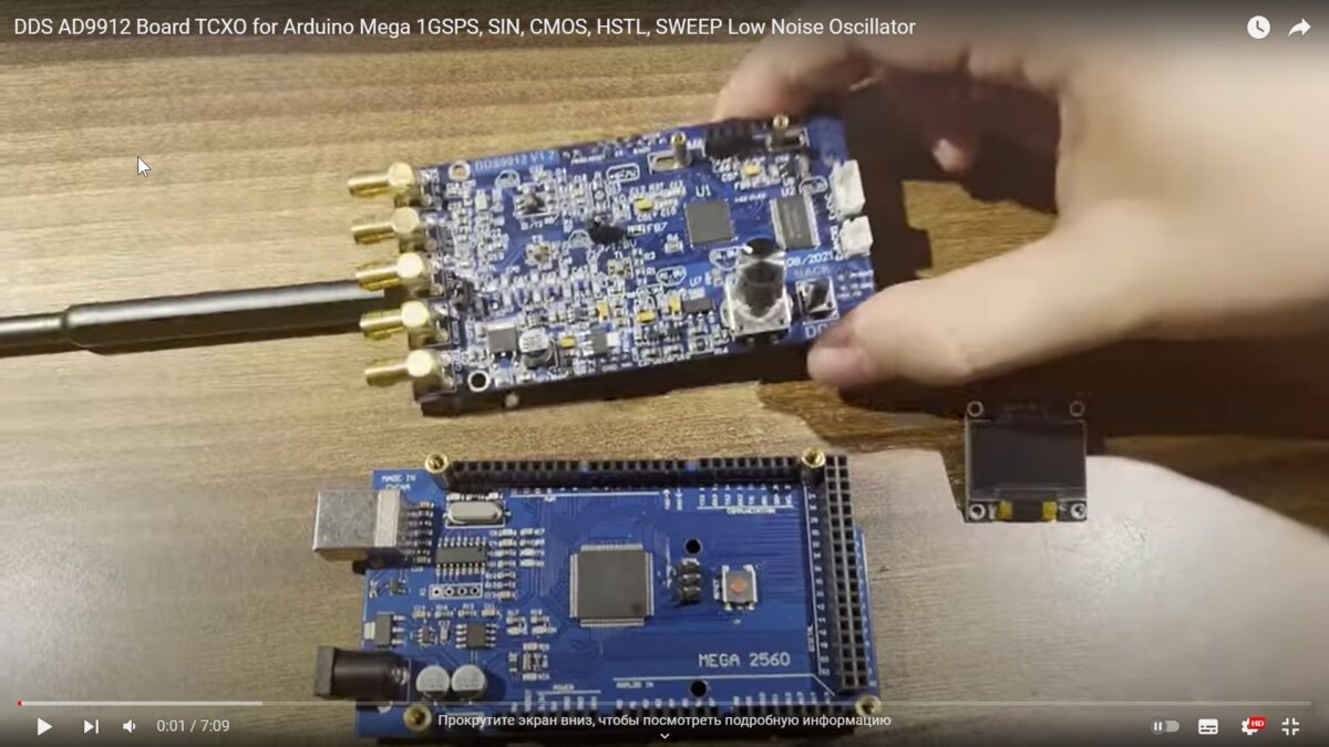
DDS Arduino Shield AD9912 RF Signal Generator by GRA & AFCH: 


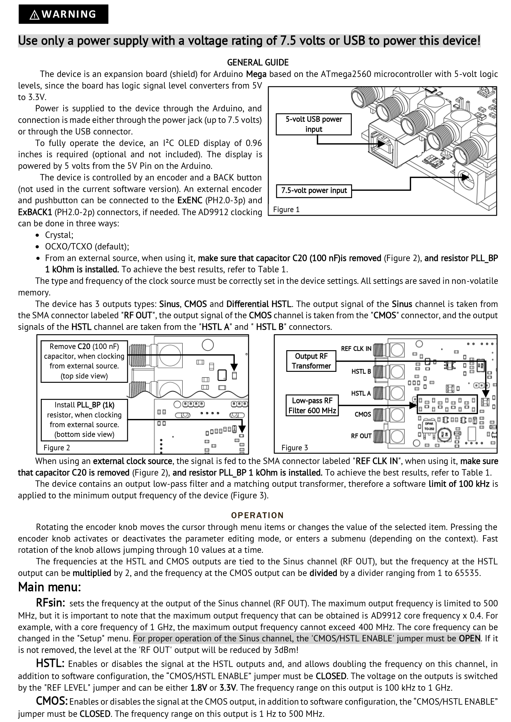
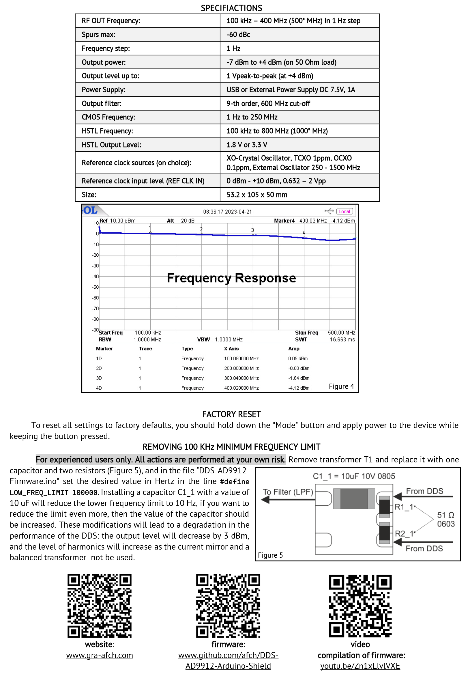
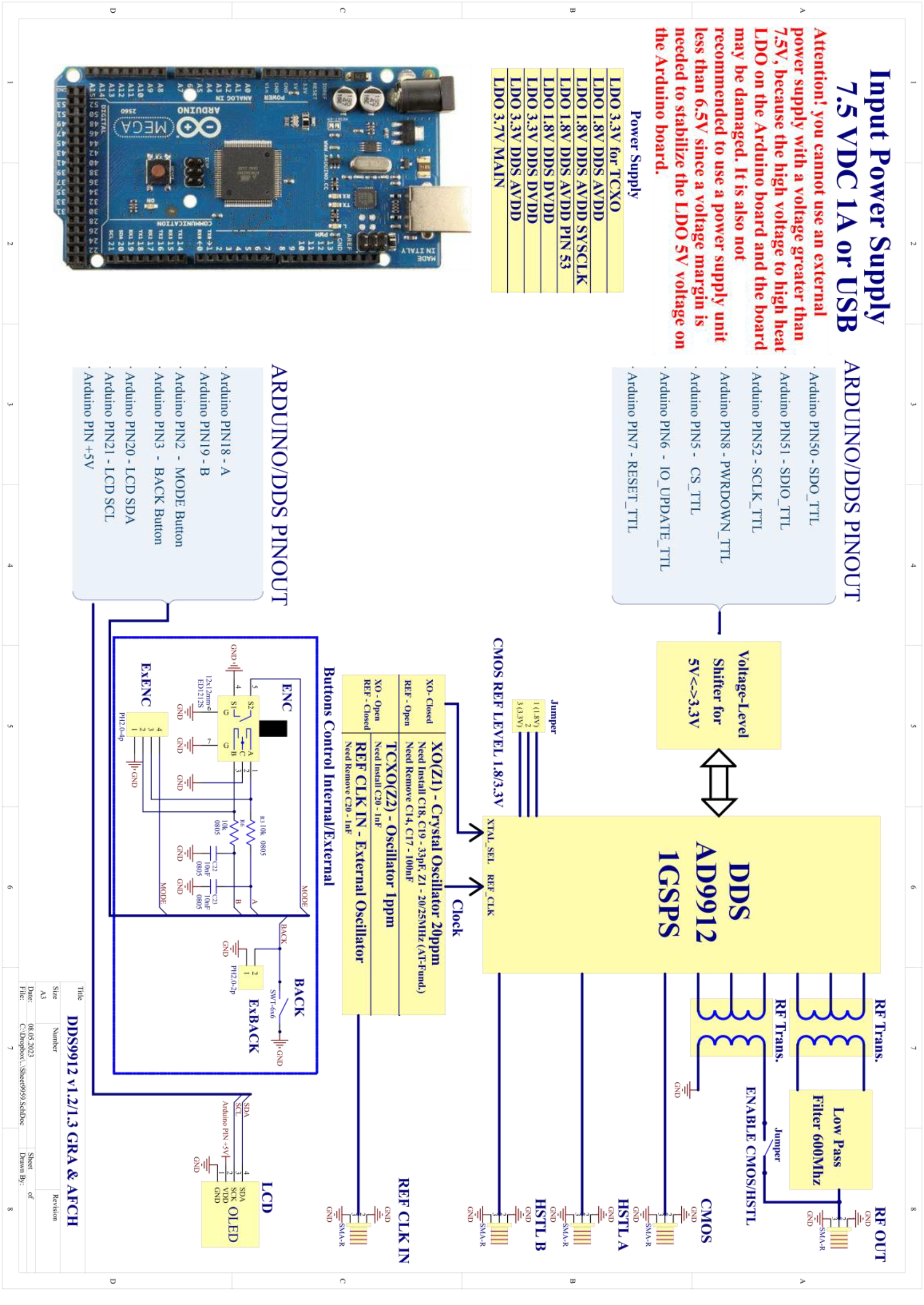
DDS AD9912 Shield Board Operating Instruction 

Operating Instruction for DDS AD9912 Shield Board v1.x (rev.B) with Connection Diagram 

DDS AD9912 Shield Board v1.x Operating Instruction (rev.B) with Connection Diagram [title]


DDS AD9912 Shield Board v1.x Operating Instruction (rev.B) with Connection Diagram [page 1]


DDS AD9912 Shield Board v1.x Operating Instruction (rev.B) with Connection Diagram [page 2]


DDS AD9912 Shield Board v1.x Operating Instruction (rev.B) with Connection Diagram [page 3]


DDS AD9912 Shield Board v1.x Operating Instruction (rev.B) with Connection Diagram [connection diagram]


Dear customers!
If you have ANY questions, (PLEASE ASK us).


Shipping and Return information


All Items are shipped from Ukraine
Via International registered Airmail
Shipments are made within 1 business day
After the payments are received and verified
It takes about 4-7 days via UPS Express delivery
It takes about 10-18 days via Standard shipping
It takes about 35-45 days via Economy shipping
We combine multiple Items to save on shipping


UPS Express Shipping time (recommended):

Europe:3-5 days
Germany:3-5 days
USA, Canada:4-7 days
Asia, South America:5-7 days
Australia, New Zealand:5-7 days
Africa, Central America:5-7 days


Standard Shipping time:

Europe:10-12 days
Germany:10-12 days
USA, Canada:10-15 days
Asia, South America:10-18 days
Australia, New Zealand:12-18 days
Africa, Central America:12-18 days


Economy Shipping time:

Europe:25-30 days
Germany:25-30 days
USA, Canada:30-35 days
Asia, South America:35-45 days
Australia, New Zealand:45-55 days
Africa, Central America:45-55 days


Return Policy

All Returns are accepted

  • For Return you should contact Us within 14 Days after receiving the Item
  • Refunds are made as Money back or Replacements (buyer’s choice)
  • Return Shipments are paid by the buyer
  • No restocking fees are charged


Dear customers!
If you have ANY questions, (PLEASE ASK us)