JLINK V9 Debugger J-LINK ARM Cortex JTAG SWD Simulation Downloader SCM
Engineers provide technical support online, for examplesomeSimulation, burn common problems
If you use Seg.It can be used with segger665 and below versions
If higher than segger665 version. There will be a pop-up window, but it can be used normally. Customers who mind should not place orders!
Supported CPUs:, ARM7/9/11, Cortex-A5/A7/A8/A9, Cortex-M0/M1/M3/M4/M7, Cortex-R4, Microchip, PIC32, and, Renesas, RX100/RX200/RX610/RX621/RX62N/RX62T/RX630/RX631/RX63N
Support mainstream ARM:STM32, ARM7, ARM9, ARM11, NXP, LPC, S3C2440, new Tang (Hua Bang), ARM, Cortex, and so on
JLink V8The difference between Jlink and V9:
1The speed is different: V8 supports up to 10M (JTAG debug mode), /4M (SWD debug mode), and Jlink V9 supports 20M (JTAG debug mode) /15M (SWD debug mode).
2The stability is different: V9 drive IC has voltage adaptive ability, in the case of proper wiring, automatically adapt to the target board CPU voltage. 1.8-5.5V's CPU can be debugged, while the V8 versionThis can only debug 3.3V versions of CPU, while debugging 5vcpu has poor stability.
3JlinkV8 easy to firmware instead of brick. I have a lot of V8 hanging here, I want to re write the firmware, and ordinary users can only look at the brick, and V9 basically no such situation.
4,Some of the latest cpuV8 is no longer supported, and V9 supports almost all ARM cpu.
JLINK, V9, six bigCharacteristic:
1 the master chip adopts STM32F205, and never firmware,Factory defaultFirmware upgrade to the latest version;
2It can provide 3.3V voltage, 0.8A current, 5V voltage, 0.5A current (first feet through jumper selection, factory default 3.3V) for the development board;
3Supports standard JTAG interface and 2 wire SWD debug interface. The speed can reach 20M (JTAG) /15M per second (SWD);
4It supports debugging of all ARM chips, supports MDK or IAR, and compiles the environment IDE supported by other standard JLink standards;
5, original firmware,Firmware automatic upgrade;
6, lead-free process, comparable to the original;

Electronic instructions and drives are downloaded via SkyDrive
Version information

Emulator comes with virtual serial port

Write, read, and erase operations using the SEGGER burn tool


Using the SEGGER J-Scope tool, you can view variable waveforms in real-time

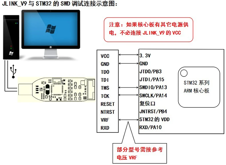
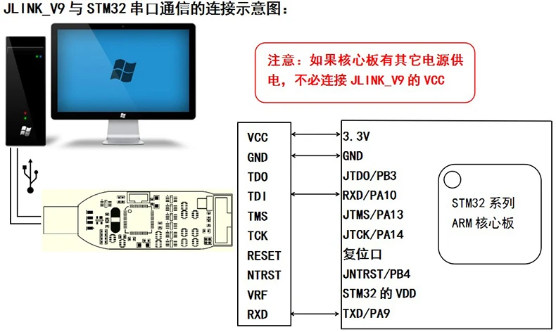
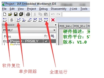
Simulation debugging method of JLINK V9 in IAR
First steps:Open the project file and select Options in the menu bar Project drop-down list to set it,
Here's an example of the IAR6.3 version, as shown in the following figure:

stayIn the Category tab, selectGeneral OptionsIn.Target select the appropriate model according to the target board chip. Here is the example of STM32F103C8TC6, as shown in the following figure:

stayIn the Category tab, select Setup, and select J-Link/J-Trace at Driver

No.2Step:stayJ-Link/J-TraceTab, select Connection, where Communication selects USB,
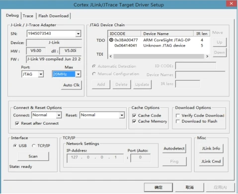
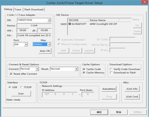
In Interface, if you use JTAG mode, select JTAG, and use SWD mode, select SWD,Select the JTAG debug mode here, as shown in the following figure:

After setting up, clickOK can go back to the project, click the simulation button, you can carry out normal simulation debugging software.
As shown in the following figure

JLINK V9 inKeil MDK simulation debuggingMethod
JTAG modeThe settings are shown in the following figure.
SWDPatternThe settings are shown in the following figure
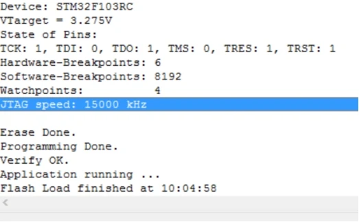
Output debug information (toSTM32F103RC as an example)