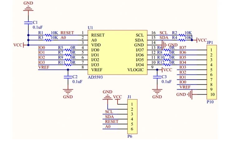
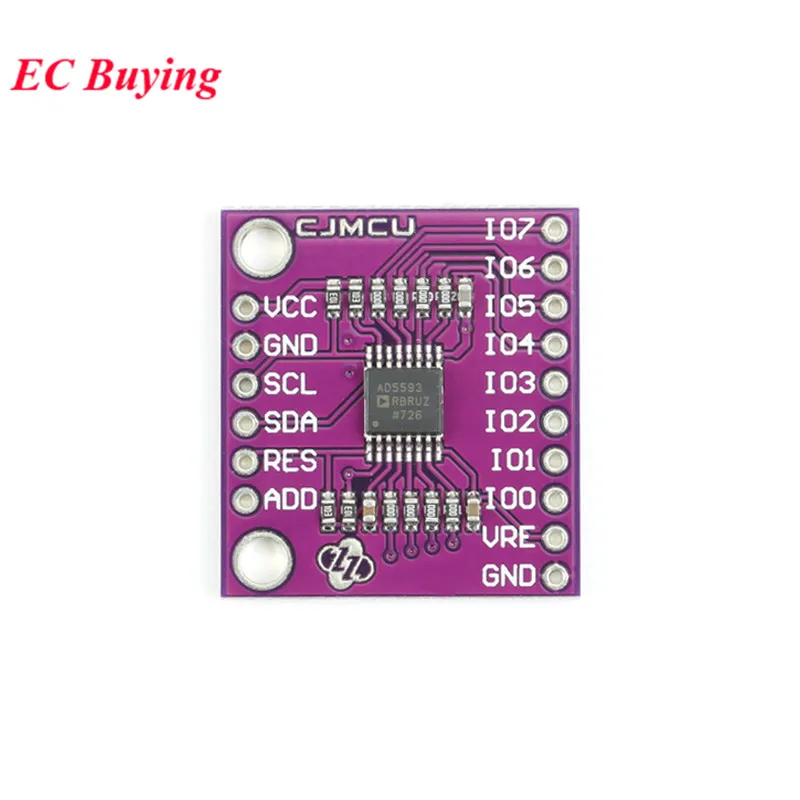
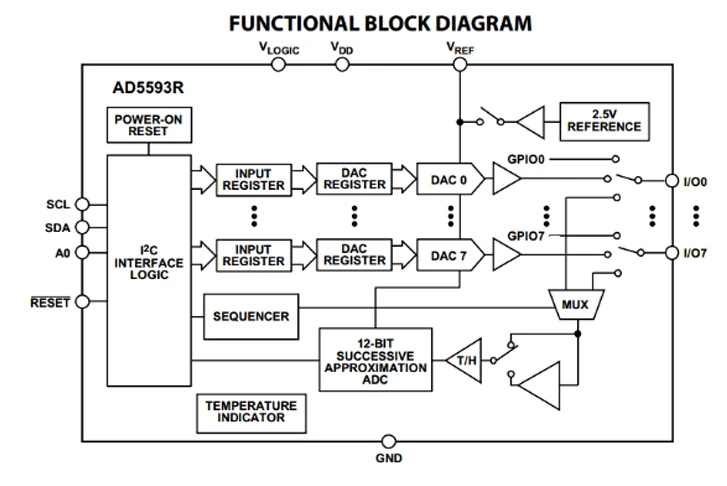
The AD5593R integrates eight I/O pins that can be individually configured as DAC outputs, ADC inputs, digital outputs, or digital inputs. When the I/O pin is configured as an analog output, it is driven by a 12-bit DAC. The DAC output range is 0 V to VREF, or 0 V to 2 x VREF. When the I/O pin is configured as an analog input, it is connected to a 12-bit ADC through an analog multiplexer. The ADC input range is 0 V to VREF, or 0 V to 2 × VREF. The I/O pins can also be configured as general purpose digital input or output (GPIO) pins. The GPIO pin status can be set or read back by accessing the GPIO registers via an I2C write/read operation. The AD5593R integrates a 2.5V, 20 ppm/°C reference (default off) and a temperature indicator (indicating chip temperature). The temperature value is read back as part of the ADC read sequence.
Parameter:
-
ADC offset error: ±5mV
-
ADC conversion time: 2us
-
ADC full power bandwidth: 8.2MHz 3dB
-
DAC offset error: ±3mV
-
DAC input full 0 error: 2mV
-
Reference voltage VREF input: 1 ~ VDD
-
Reference voltage VREF output: 2.5V
-
Temperature sensor accuracy: 12 bits
-
Temperature sensor temperature range: -40 ~ 105 ° C
-
Measurement error: ±3 °C
-
Power supply VDD: 2.7 ~ 5V
-
IIC communication frequency: up to 400KHz
-
VCC: Positive power supply
-
SCL: IIC clock signal line
-
SDA: IIC data signal line
-
/RES: Chip reset terminal, active low
-
ADD: 7-bit slave address minimum selection bit
-
IO0 to IO7: Octal digital or analog signal input/output (internal register setting)
-
VRE: Reference voltage input and output (when the internal setting is enabled). When the internal is not enabled, an external reference voltage of 1V to VCC is required.