EI-OT ESP8266 Tasmota ESPEasy ESP-07S Entwicklerplatine Bausatz Set

EI-OT ESP8266 Tasmota ESPEasy ESP-07S 5-12V Entwicklerplatine Development Board ADC adj. Pull Down Up Kit Set

EI-OT ESP8266 ESP-07S Development Board Set © ei-ot ®

EI-OT ESP8266 ESP-07S 5-12V Development Board Set © ei-ot ®

EI-OT ESP8266 Development Board Dimesnions © ei-ot ®

EI-OT ESP8266 Development Board Module Assembling © ei-ot ®

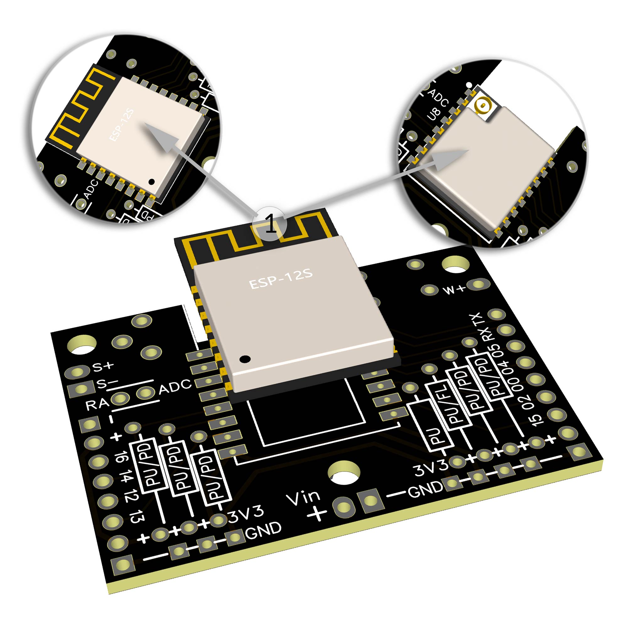
EI-OT ESP8266 Development Board Pin Header Assembling © ei-ot ®


EI-OT ESP8266 Development Board Voltage Divider Reset Button assembling © ei-ot ®

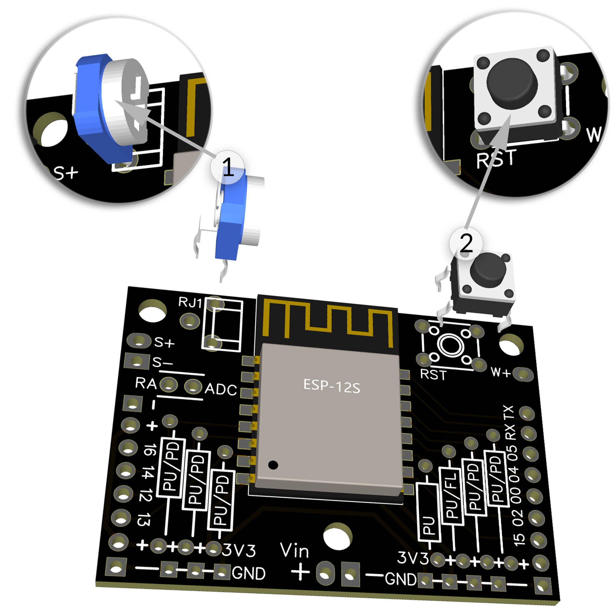
EI-OT ESP8266 Development Board 5-12V Power Supplyconnecting © ei-ot ®

EI-OT ESP8266 Development Board Pull Up Pull Down Resistors © ei-ot ®


EI-OT ESP8266 Development Board ADC Voltage Divider © ei-ot ®


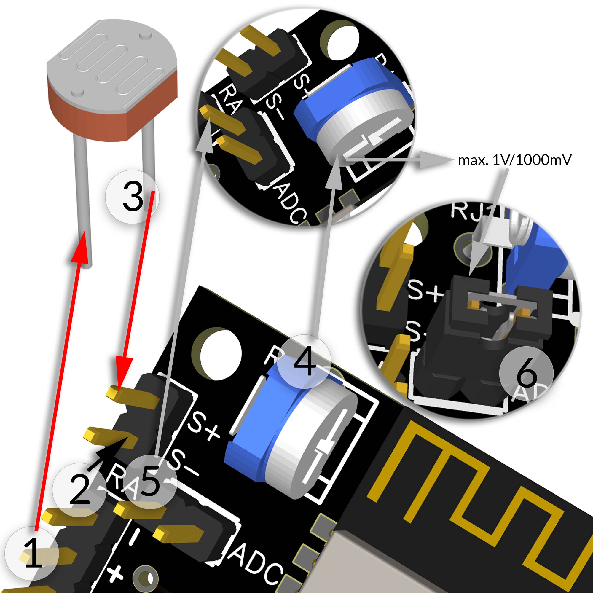
Unsere EI-OT ESP8266 Entwicklerplatine im Set mit dem ESP8266 ESP-07S Modul ist wie folgt verfügbar

  • ESP-07S Standard mit Espressif AT Firmware
  • ESP-07S Tasmota mit Tasmota Firmware (tasmota-4M.bin) 1
  • ESP-07S ESPEasy mit ESPEasy Firmware (ESP_Easy_mega_normal_ESP8266_4M1M) 1
  •  

    1 Die Tasmota und ESPEasy Firmware ist stets in englischer Sprache und eignet sich um bei Bedarf die individuelle Firmware mittels OTA Update zu installieren, es wird kein USB TTL Konverter benötigt.

     
    ESP8266 ESP-07S

    Der ESP-12 Modul basiert auf der ESP8266EX MCU und verfügt über einen 32Mbit Flash Speicher, 64Kb Instruction Ram und 96Kb Data Ram. Je nach installierter Firmware können die GPIO's als

    • digitale Ein- oder Ausgänge
    • Schnittstelle wie
      • UART (GPIO1 und GPIO3)
      • SPI
      • I2C
      • 1wire
      • usw.
    konfiguriert werden. Zusätzlich verfügt der ESP12-S über einen analogen Signaleingang (GPIO17) in Kombination mit einem Analog - Digital - Converter.
     
    EI-OT ESP8266 Entwicklerplatine

    Im Vergleich zu typischen ESP8266 Entwicklerplatinen wurde die EI-OT ESP8266 Entwicklerplatine für einen weitreichenden praktischen Einsatz konzipiert. Bereits bei der Spannungsversorgung wird ein TLE42744GSV33 von Infineon verwendet. Diesbezüglich erlaubt das  EI-OT ESP8266 Modul Spannungsversorgungen von 5-12V bei bis zu 400mA. Neben der typischen Ausführung der GPIO's auf Stiftleisten (im Abstand von 2,54 mm angeordnet) stehen zusätzlich 3,3V Ausgänge zur Spannungsversorgung von beispielsweise Sensoren bereit.

     
    analoger Signaleingang

    Neben den digitalen GPIO's verfügt die EI-OT ESP8266 Entwicklerplatine über einen analogen Signaleingang in Kombination mit einem variablen Spannungsteiler. Im Detail können analoge Eingangssignale mittels Potentiometer, individuell auf den ADC Eingang des ESP8266 eingestellt werden.

     
    Pull Up & Pull Down Widerstände

    Beim Einsatz der ESP8266 GPIO's bedarf es typischerweise einem Pull Up oder Pull Down Widerstand. Die EI-OT ESP8266 Entwicklerplatine verfügt über entsprechende Kontakte um

    • GPIO00
    • GPIO02
    • GPIO04
    • GPIO05
    • GPIO12
    • GPIO13
    • GPIO14
    um mit einem Widerstand zu beschalten.
     
    Firmware

    Der Funktionsumfang der EI-OT ESP8266 Entwicklerplatine wurde strikt den typischen und grundlegendem Funktionsprinzip des ESP8266EX angelehnt.

    • CH_EN Chip Enable ist bereits mit +3,3V beschaltet
    • GPIO15 verfügt über einen Pull Down Widerstand / Boot from Flash
    • GPIO00 kann bei Bedarf Low beschaltet werden / Flash Modus
    Die EI-OT ESP8266 Entwicklerplatine eignet sich somit für eigene Firmware Entwicklung als auch Firmware basierend auf
    • Espressif NonOS AT
    • Arduino
    • NodeMCU
    • MicroPython
    • Tasmota
    • ESPEasy
    • ESPurna
    • usw.
     
    Die ESP8266 Entwicklerplatine
    ist bereits auf der Rückseite mit grundlegende SMD Komponenten wie
    • TLE42744GSV33 Spannungskonverter
    • 4 Stück Kondensatoren
    • Widerständen
    bestückt.
     
    EI-OT ESP8266 Entwicklerplatine Bausatz Lieferumfang
    Neben der Hauptplatine sind im EI-OT ESP8266 Entwicklerplatinen Bausatz folgende Komponenten enthalten:
    • 1 Stück ESP-07S Modul
    • 4 Stück 10KΩ Widerstände bedrahtet 1%
    • 3 Stück 4,7KΩ Widerstände bedrahtet 1%
    • 1 Stück 6x6 Reset Taster
    • 1 Stück Pinleiste gelb 8-polig
    • 1 Stück Pinleiste gelb 9-polig
    • 2 Stück Pinleiste blau 2-polig
    • 1 Stück Pinleiste rot 2-polig
    • 1 Stück Jumper für Spannungsteiler
    • 1 Stück RM063 Potentiometer
     

    ESP8266 ESP-07S Entwicklerplatine für 5-12V VCC optimiert für den praktischen Einsatz

     
    GPIO und weitere Anschlüsse
    Bei der ESP8266 Entwicklerplatine wurde folgende Anschlüsse auf Pins (2,54mm raster) ausgeführt
    • Pinleiste gelb 9-polig
      1. TX
      2. RX
      3. GPIO05
      4. GPIO04
      5. GPIO00
      6. GPIO02
      7. GPIO15
      8. + 3,3V
      9. - GND
    • Vin Pinleiste rot 2-polig
      1. - GND
      2. + 5-12Vcc
    • Pinleiste gelb 8-polig
      1. - GND
      2. + 3,3V
      3. GPIO16
      4. GPIO14
      5. GPIO12
      6. GPIO13
      7. + 3,3V
      8. - GND
    • Pinleiste blau 2-polig
      1. S+ analoger Signaleingang
      2. S- GND analoger Signaleingang
    • Pin-/ Jumper- Leiste blau 2-polig
      1. RA + variabler Signaleingang Spannungsteiler
      2. ADC analoger Signaleingang ESP8266
     

    Our EI-OT ESP8266 developer board in set with ESP8266 ESP-07S module is available as follows

  • ESP-07S default with Espressif AT firmware
  • ESP-07S Tasmota with Tasmota Firmware (tasmota-4M.bin) 1
  • ESP-07S ESPEasy with ESPEasy Firmware (ESP_Easy_mega_normal_ESP8266_4M1M) 1
  •  

    1 The Tasmota and ESPEasy firmware is always in English and is suitable for installing the individual firmware using OTA update function, - no USB TTL converter is required -  

    ESP8266 ESP-07S
    The ESP-12 Module is based on the ESP8266EX MCU and features 32Mbit Flash memory, 64Kb Instruction Ram and 96Kb Data Ram. Depending on the installed firmware, the GPIO's can be used as
    • digital inputs or outputs
    • interface like
      • UART (GPIO1 and GPIO3)
      • SPI
      • I2C
      • 1wire
      • etc.
    The ESP12-S has also an analog signal input (GPIO17) in combination with an analog - digital - converter.
     
    EI-OT ESP8266 Development Board

    Compared to typical ESP8266 developer boards, the EI-OT ESP8266 developer board is designed for wide-ranging practical use. A TLE42744GSV33 from Infineon is already used for the power supply. In this regard, the EI-OT ESP8266 module allows power supplies of 5-12V @ up to 400mA. In addition to the typical design of the GPIOs on pin strips (arranged at a distance of 2.54 mm), there are also 3.3V outputs available for the power supply of sensors, for example.


    analog signal input
    In addition to the digital GPIO's, the EI-OT ESP8266 developer board has an analog signal input in combination with a variable voltage divider. In detail, analog input signals can be adjusted individually to the ADC input of the ESP8266 using a potentiometer.
       
    Pull Up & Pull Down Resistors
    When using the ESP8266 GPIO's, a pull up or pull down resistor is typically required. The EI-OT ESP8266 developer board has corresponding contacts around
    • GPIO00
    • GPIO02
    • GPIO04
    • GPIO05
    • GPIO12
    • GPIO13
    • GPIO14
    to connect GPIO with a resistor
     
    Firmware
    The range of functions of the EI-OT ESP8266 developer board was strictly based on the typical and basic functional principle of the ESP8266EX.
    • CH_EN Chip Enable is already connected to +3.3V
    • GPIO15 has a pull down resistor / boot from flash
    • GPIO00 can be wired low if required / flash mode
    The EI-OT ESP8266 developer board is therefore suitable for your own firmware development as well as firmware based on
    • Espressif NonOS AT
    • Arduino
    • NodeMCU
    • MicroPython
    • tasmota
    • ESPEasy
    • ESPurna
    • etc.
     
    The ESP8266 Development Board
    is already assembled with SMD components
    • TLE42744GSV33 voltage converter
    • 4 pcs. capacitors
    • resistors
       
    The EI-OT ESP8266 Development Board Kit scope of delivery
    In addition to the main board, the following components are included in the EI-OT ESP8266 developer board kit :
    • 1 Stück ESP-07S Module
    • 4 pcs. 10KΩ Resistor 1%
    • 3 pcs. 4.7KΩ Resistor 1%
    • 1 pcs. 6x6 Reset Button
    • 1 pcs. Pinheader 1-row 8-pole yellow
    • 1 pcs. Pinheader 1-row 9-pole yellow
    • 2 pcs. Pinheader 1-row 2-pole blue
    • 1 pcs. Pinheader 1-row 2-pole red
    • 1 pcs. Jumper for Voltage Divider
    • 1 pcs. RM063 Potentiometer
         

    ESP8266 ESP-07S developer board for 5-12V VCC optimized for practical use

     
    GPIO and additionally Connections
    The ESP8266 developer board has the following connections on pins (2.54mm pitch).
    • Pinheader yellow 9-Pin
      1. TX
      2. RX
      3. GPIO05
      4. GPIO04
      5. GPIO00
      6. GPIO02
      7. GPIO15
      8. + 3,3V
      9. - GND
    • Vin Pinheader red 2-Pin
      1. - GND
      2. + 5-12Vcc
    • Pinheader yellow 9-Pin
      1. - GND
      2. + 3,3V
      3. GPIO16
      4. GPIO14
      5. GPIO12
      6. GPIO13
      7. + 3,3V
      8. - GND
    • Pinheader blue 2-Pin
      1. S+ analog signal input
      2. S- GND analog signal input
    • Pinheader Jumper blue 2-Pin
      1. RA + adjustable signal input voltage divider
      2. ADC analog signal input ESP8266
     
    EI-OT ESP8266 ESP-07S Development Board Set Features
    VCC Spannungsversorgung DC 5-12V  VCC  / Input Voltage DC 5-12V
    Schnittstellen je nach GPIO Konfiguration Interfaces based on GPIO configuration
    Protokolle HTTP, REST, MQTT, Domoticz, Home Assistant Protocols HTTP, REST, MQTT, Domoticz, Home Assistant
    typische Anwendung ESP8266 Entwicklerplatine typical Application  ESP8266 Development Board
    Leistung Strom Power Current
    TLE42744GSV33 Ausgangsstrom 400mA (max.) TLE42744GSV33 Output Current 400mA (max.)
    Stromverbrauch (ESP8266 Modul nicht enthalten)

    60mA (durchschnittlich)
    200mA (max.)
    23mA (Modem Sleep)
    5mA (Light Sleep)
    <3mA (Deep Sleep)

    Current Consumption (ESP8266 Module not included)

    60mA (average)
    200mA (max.)
    23mA (Modem Sleep)
    5mA (Light Sleep)
    <3mA (Deep Sleep)

    WLan 802.11 WiFi 802.11
    Frequenzbereich 2412 - 2884 Mhz. Frequency Range 2412 - 2884 Mhz.
    Sendeleistung 802.11b: 16±2 dBm (@11Mbps)
    802.11g: 14±2 dBm (@54Mbps)
    802.11n: 13±2 dBm (@HT20, MCS7)
    Transmit Power 802.11b: 16±2 dBm (@11Mbps)
    802.11g: 14±2 dBm (@54Mbps)
    802.11n: 13±2 dBm (@HT20, MCS7
    Empfangs - Empfindlichkeit CCK, 1 Mbps : -90dBm
    CCK, 11 Mbps: -85dBm
    6 Mbps (1/2 BPSK): -88dBm
    54 Mbps (3/4 64-QAM): -70dBm
    HT20, MCS7 (65 Mbps, 72.2 Mbps): -67dBm
    Receiving Sensitivity CCK, 1 Mbps : -90dBm
    CCK, 11 Mbps: -85dBm
    6 Mbps (1/2 BPSK): -88dBm
    54 Mbps (3/4 64-QAM): -70dBm
    HT20, MCS7 (65 Mbps, 72.2 Mbps): -67dBm
    Sicherheit WEP/WPA-PSK/WPA2-PSK Security WEP/WPA-PSK/WPA2-PSK
    Antenne externe Antenne I-PEX UFL Anschluss (ESP-07S) Antenna extrenal Antenna I-PEX UFL Connector (ESP-07S)
    IPv4 Unterstützung DHCP und statisch IPv4 Support DHCP and static
    Anschlüsse Connections
    Vin Pinleiste rot 2-polig 5-12V Spannungsversorgung (Vin / GND) Vin Pinheader red 2-pole 5-12V Power Supply (Vin / GND)
    Pinleiste gelb 8-polig - GND
    + 3,3V
    GPIO16
    GPIO14
    GPIO12
    GPIO13
    + 3,3V
    - GND
    Pinheader yellow 8-pole - GND
    + 3.3V
    GPIO16
    GPIO14
    GPIO12
    GPIO13
    + 3.3V
    - GND
    Pinleiste gelb 9-polig TX
    RX
    GPIO05
    GPIO04
    GPIO00
    GPIO02
    GPIO15
    + 3,3V
    - GND
    Pinheader yellow 9-pole TX
    RX
    GPIO05
    GPIO04
    GPIO00
    GPIO02
    GPIO15
    + 3.3V
    - GND
    Pinleiste blau 2-polig S+ analoger Signaleingang
    S- GND analoger Signaleingang
    Pinheader blue 2-pole S+ analog signal input
    S- GND analog signal input
    RA ADC Pinleiste / Jumper blau 2-polig RA + variabler Signaleingang Spannungsteiler
    ADC analoger Signaleingang ESP8266
    RA ADC Pinheader / Jumper blue 2-pole RA + adjustable signal input voltage divider
    ADC analog signal input ESP8266
    EI-OT ESP8266 Development Board ESP-07S ESP-07S Module assembling
    ESP8266 bestücken
    Die EI-OT ESP8266 Entwicklerplatine ist bereits mit SMD Komponenten auf der Rückseite bestückt. Zur Inbetriebnahme müssen nachfolgende Komponenten wie in nebenstehender Grafik (zum Vergrößern auf das Bild klicken) bestückt / verlötet werden Die Bestückung der EI-OT ESP8266 Entwicklerplatine Schritt für Schritt:
    1. Das ESP8266 Modul entsprechend platzieren, am besten mit einem Clip, z.B. Wäscheklammer fixieren und verlöten
    ESP8266 Assembling
    Besides the SMD components on bottom side of PCB, the EI-OT ESP8266 Development Break Out Module requires additional components. Assembling of the 16 Channel PRO Relays Module Step by Step:
    1. Put the ESP8266 Module in correct direction on position, fix it with a clip or clothes peg and solder it.
    2. Put the 6-pole Pinheader on J1 and solder the Pins from backside
    3. Put the 2-pole Pinheader on A2 A1 and solder the Pins from backside
    The basic assembling of the EI-OT 16 Channel PRO Relays Module is finished.
    EI-OT ESP8266 Dev.-Kit ADC Potentiometer RST Button assembling
    Poti Taster bestücken
    Nachdem das ESP8266 LED Controller Modul mit dem ESP8266 bestückt wurde müssen der Potentiometer und der Reset Taster wie folgt bestückt werden:
    1. Platziere das RM063 Potentiometer auf RJ1 und verlöte die Pins auf der Rückseite
    2. Platziere den 6x6 Taster auf RST und verlöte die Pins auf der Rückseite
    Poti Button Assembling
    After assembling ESP8266 module on EI-OT ESP8266 Break Out Board, Reset Button and ADC Potentiometer must be assembled:
    1. Put the RM063 Potentiometer on RJ1 and solder the Pins from backside
    2. Put the 6x6 Button RST and solder the Pins from backside
    EI-OT ESP8266 LED Stripe Controller TO220  assembling
    Stiftleisten  bestücken
    Zur besseren Differenzierung  umfasst der Lieferumfang des EI-OT ESP8266 Entwicklerkit farbige Pinleisten
    • gelb, seitliche Anschlüsse (GPIO's und 3,3V Spannungsausgang)
    • rot, Spannungsversorgung (5-12V)
    • blau, ADC Anschluß sowie ADC Brücke / Jumper
    BITTE VOR DEM BESTÜCKEN die entsprechende Farbe der Pinleiste berücksichtigen
    1. Platziere die 9-polige gelbe Pinleiste und verlöte die Pins auf der Rückseite
    2. Platziere die 2-polige rote Pinleiste und verlöte die Pins auf der Rückseite
    3. Platziere die 8-polige gelbe Pinleiste und verlöte die Pins auf der Rückseite
    4. Platziere die 2-polige blaue Pinleiste und verlöte die Pins auf der Rückseite
    5. Platziere die 2-polige blaue Pinleiste und verlöte die Pins auf der Rückseite
    Die EI-OT ESP8266 Entwicklerplatine ist nun betriebsbereit und kann angeschlossen werden.
    Pinheader Assembling
    For better differentiation, the scope of delivery of the EI-OT ESP8266 developer kit includes colored pin strips
    • yellow, side connections (GPIO's and 3.3V voltage output)
    • red, power supply (5-12V)
    • blue, ADC connection and ADC bridge / jumper
    PLEASE consider the corresponding color of the pin strip BEFORE ASSEMBLING
    1. Place the 9-pin yellow pin header and solder the Pins from backside
    2. Place the2-pin red pin header and solder the Pins from backside
    3. Place the 8-pin yellow pin header and solder the Pins from backside
    4. Place the 2-pin blue pin header and solder the Pins from backside
    5. Place the 2-pin blue pin header and solder the Pins from backside
    The EI-OT ESP8266 developer board is now assembled and can be connected.
    ESP8266 Development Board 5-12V Power Supply connection
    Spannungsversorgung
    Die EI-OT ESP8266 Entwicklerplatine verfügt über einen AMS1117 Spannungskonverter und erlaubt Versorgungsspannungen von 5VDC bis 12VDC. Die Spannungsversorgung der EI-OT ESP8266 Entwicklerplatine erfolgt zentral über Vin 2 -polige, rote Pinleiste. Beim Anschluss muss stets auf + und - geachtet werden, ein falscher Anschluß führt zu Beschädigung der ESP8266 Entwicklerplatine.
    Power Supply
    The EI-OT ESP8266 developer board has an AMS1117 voltage converter and allows supply voltages from 5VDC to 12VDC. The power supply of the EI-OT ESP8266 developer board is done centrally thru Vin 2-pin, red pinheader. When connecting, always pay attention to + and -, incorrect connection will damage the ESP8266 developer board.
    Pull Up Pull Down Widerstand
    Als typische MCU (MikroController Unit) verfügt der ESP8266 über GPIO's (General Purpose Input/Output). Mit einfachen Worten ein Pin / Kontakt der individuell und anwendungsspezifisch genutzt werden kann, beispielsweise als
    • digitaler Eingang, mit High +3,3V und Low Level GND
    • Schnittstelle, 1-Wire oder im Verbund als Anschluss einer Schnittstelle als MOSI, MISO, CS, CLK, ....
    Neben den individuell nutzbaren GPIO's verfügt der ESP8266 auch über folgende GPIO's die für interne Funktionen benötigt werden beispielsweise
    • GPIO0 Low/GND Flash Modus aktiv High/3,3V+ Boot Modus aktiv
    • GPIO15 Low/GND bootet vom SPI Flash High/3,3V+ bootet von einer SD Speicherkarte
    Je nach Verwendung und Funktion eines GPIO bedarf es in der Regel (fast ausnahmslos) eines
    • Pull Up Widerstand, der zwischen 3,3V+
    • Pull Down Widerstand, der zwischen GND
    und dem jeweiligen GPIO geschaltet wird. Die EI-OT ESP8266 Entwicklerplatine ist dementsprechend vorbereitet um bei Bedarf einen GPIO mit einem notwendigen Widerstand zu beschalten.
    Pull Up Pull Down Widerstand
    As a typical MCU (microcontroller unit), the ESP8266 has GPIOs (General Purpose Input/Output). In simple words, a pin / contact that can be used individually and application-specifically, for example as a
    • digital input, with high +3.3V and low level GND
    • Interface, 1-Wire or in combination as connection of an interface as MOSI, MISO, CS, CLK, ....
    In addition to the individually usable GPIO's, the ESP8266 also has the following GPIO's that are required for internal functions, for example
    • GPIO0 Low/GND flash mode active High/3.3V+ boot mode active
    • GPIO15 Low/GND boots from the SPI Flash High/3.3V+ boots from an SD memory card
    Depending on the use and function of a GPIO, usually a
    • Pull up resistor between 3.3V+
    • Pull down resistor between GND
    and the respective GPIO is required. The EI-OT ESP8266 developer board is prepared accordingly to connect a GPIO with a resistor if necessary.
    ESP8266 Development Board Pull Up Pull Down Resistor connection
    Pull Up anschliessen

    Bitte stets auf entsprechenden Abstand zwischen Platine und Widerstand achten um einen Kurzschluss zu vermeiden

    1. platziere  einen Kontakt des bedrahteten Widerstand im jeweiligen GPIO Anschluss der EI-OT ESP8266 Entwicklerplatine und verlöte den Kontakt
    2. platziere den zweiten Kontakt des bedrahteten Widerstand an einem + 3V3 Anschluss der EI-OT ESP8266 Entwicklerplatine und verlöte den Kontakt
    Pull Down anschliessen

    Bitte stets auf entsprechenden Abstand zwischen Platine und Widerstand achten um einen Kurzschluss zu vermeiden

    1. platziere  einen Kontakt des bedrahteten Widerstand im jeweiligen GPIO Anschluss der EI-OT ESP8266 Entwicklerplatine und verlöte den Kontakt
    2. platziere den zweiten Kontakt des bedrahteten Widerstand an einem - GND Anschluss der EI-OT ESP8266 Entwicklerplatine und verlöte den Kontakt
    Pull Up connection

    Bitte stets auf entsprechenden Abstand zwischen Platine und Widerstand achten um einen Kurzschluss zu vermeiden

    1. place a contact of the wired resistor in the respective GPIO connection of the EI-OT ESP8266 developer board and solder the contact
    2. place the second contact of the wired resistor to a + 3V3 terminal of the EI-OT ESP8266 developer board and solder the contactConnection of the LDR is complete.
    Pull Down connection

    1. place a contact of the wired resistor in the respective GPIO connection of the EI-OT ESP8266 developer board and solder the contact
    2. place the second contact of the wired resistor to a - GND terminal of the EI-OT ESP8266 developer board and solder the contact
    ESP8266 ADC Eingang
    Der ESP8266 verfügt am GPIO17 über einen analogen Signaleingang. Mittels einem ADC (Analog Digital Converter) werden analoge Spannungswerter auf einen digitalen Wert von 0 bis 1023 umgesetzt. Der ESP8266 unterstützt dabei maximal 1000mV am ADC Signaleingang. Signalwerte über 1V  können zu Beschädigung des ESP8266 führen. Diesbezüglich verfügt die EI-OT ESP8266 Entwicklerplatine über einen variablen, mittels Potentiometer einstellbaren Spannungsteiler, um den maximalen Signalwert individuell zu begrenzen. Die Verwendung, Anschluss und Einstellung wird nachfolgend am Beispiel eines einfachen LDR (lichtempfindlichen Widerstand) beschrieben. Selbstredend bedarf es einem Multimeter zur Messung von Gleichspannung um die Signalspannung entsprechend zu limitieren!
    ESP8266 ADC Input
    The ESP8266 has an analog signal input on  GPIO17. The GPIO17 has an ADC (Analog Digital Converter), to convert analog voltage values to a digital values from 0 to 1023. The ESP8266 supports a maximum of 1000mV at the ADC signal input. Signal values ​​above 1V can damage the ESP8266. In this regard, the EI-OT ESP8266 developer board has a variable voltage divider that can be set using a potentiometer in order to individually limit the maximum signal value. Typical application, connection and setup is described below, using a simple LDR (Light Dependent Resistor) as an example. Of course you need a multimeter to measure DC voltage in order to limit the signal voltage accordingly.
    ESP8266 RGBW Module RGB LED and Power Supply connection
    LDR anschliessen
    Vor Beginn stelle sicher dass
    • keine Spannungsversorgung an der EI-OT Entwicklerplatine anliegt
    • der Jumper RA ADC nicht gesetzt ist
    Das Funktionsprinzip eines LDR ist sehr einfach, je stärker der Lichteinfall desto niedriger der Widerstand und somit die Ausgangsspannung. Dementsprechend wird der LDR über die EI-OT ESP8266 Entwicklerplatine mit 3,3V+ versorgt.
    1. Klemme hierzu einen Pin des LDR an den + Pin der EI-OT ESP8266 Entwicklerplatine
    2. Des Weiteren muss der Spannungsteiler mit GND verbunden werden, klemme hierzu den - Pin der EI-OT ESP8266 Entwicklerplatine auf den S- Pin der 2-poligen blauen Pinleiste
    3. Der verbleibende Pin des LDR gibt die auszuwertende Signalspannung die mittels ADC auf einen digital Wert umgesetzt wird. Die positive Signalspannung muss nun mit dem Spannungsteiler der  EI-OT ESP8266 Entwicklerplatine verbunden werden, klemme hierzu die LDR Signalspannung auf den S+ Pin der 2-poligen blauen Pinleiste
    Der Anschluss des LDR ist abgeschlossen.
    Signalspannung einstellen
    Vor Beginn stelle sicher dass
    • der Jumper RA ADC nicht gesetzt ist
    • wie bereits erwähnt ein Multimeter zur Messung der Signalspannung zur Hand ist
    Versorge die EI-OT ESP8266 Entwicklerplatine mit Spannung. Die Ausgangsspannung des Spannungsteiler (Signalspannung) liegt nun am Pin RA (Resistor Adjust) an. 4. Mittels dem Potentiometer kann nun die Signalspannung (Pin RA) entsprechend variiert werden 5. Um die aktuelle Signalspannung zu messen muß lediglich die positive Prüfspitze des Multimeters mit Pin RA und die negative Prüfspitze mit GND verbunden werden 6. Sobald die Signalspannung / Ausgangsspannung des Spannungsteilers eingestellt (auf max. 1000mV limitiert) wurde, muss der Jumper auf RA und ADC gesetzt werden, sodass der ADC des ESP8266 ein digitales Signal ausgibt.
    LDR connection
    Before you start, make sure
    • There is no power supply connected to the EI-OT ESP8266 Development Board
    • the jumper RA  ADC is not set
    A LDR is a passive component that decreases resistance with respect to receiving luminosity (light) and increases signal voltage. Accordingly, the LDR is supplied with 3.3V+ via the EI-OT ESP8266 Development Board.
    1. in this regard connect one pin of the LDR to the + pin of the EI-OT ESP8266 Development Board.
    2. the voltage divider requires also a GND, connect the - pin of the EI-OT ESP8266 Development Board to the S- Pin of the blue 2-pole pinheader
    3. The second pin of the LDR is the signal voltage output to be evaluated, which is converted to a digital value using an ADC. This positive signal voltage must be connected to the voltage divider of the EI-OT ESP8266 Development Board.In this regard connect the LDR signal voltage Pin to the S+ Pin of the blue 2-pole Pinheader
    Connection of the LDR is complete.
    Signal voltage adjustment
    Before you start, make sure
    • the jumper RA ADC is not set
    • as already mentioned, a multimeter is available to measure the signal voltage
    Supply the EI-OT ESP8266 Development Board with voltage. The output voltage of the voltage divider (Signal Voltage) is now present at Pin RA. 4. The signal voltage (Pin RA) can now be varied thru the potentiometer 5. To measure the current signal voltage, you only have to connect the positive test tip of the multimeter to Pin RA and the negative test tip to GND 6. Once the signal voltage / output voltage of the voltage divider has been set / limited to max. 1000mV, the jumper must be placed on RA and ADC to forward signal voltage to ESP8266 ADC.