Highlights:
Our shop is introducing many kinds of phase-locked loops, especially an integrated VCO phase-locked loop of ADF43504351 series with high performance-price ratio, which is convenient for developers to develop and use for the second time. It has a great guarantee in parameter design and test.
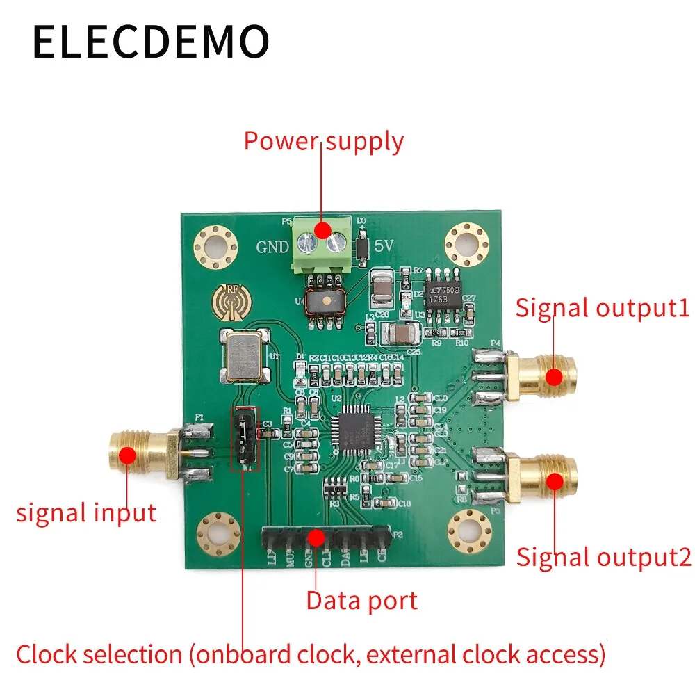
ADF4351 module shipping list
Module + PDF schematic diagram + routine source code + after-sale technical support + electrostatic bag packaging + shockproof foam
Tips:
(1) The module interface of our shop is clear and the performance is stable. Please perform functional verification under the corresponding experimental conditions in conjunction with the schematic diagram provided by our shop.
(2) The basic parameters of this module are in the details page, providing PDF information of the module information and source code of the routine; engineering files are not provided, please be clear to the buyer, if you have any operation problems, please consult customer service.
(3) Buyers, before using the module, please read the details page of this module to understand the power supply and use restrictions, to avoid damage to the module due to improper operation.
(4) Our store modules are guaranteed to provide real module parameters, functions and pictures, and all module j will be shipped after detection.
Please contact customer service after purchase, we will send the module information to your mailbox.
Module parameters
Module model: ADF4351
Module type: broadband PLL frequency source
Power supply voltage: DC-5V
Module current: 160mA (MAX); quiescent current 20mA (TYP) normal drive current (155mA)
Module communication protocol: SPI
Module provides routines: STM32F103RBT6; point frequency, frequency sweep
Routine platform: STM32F103X-M3; KEIL5 version source code
Module reference frequency: 100MHz; clock can be input externally
Reference frequency signal amplitude: 700mVpp(MIN)
Frequency stability: greater than 25PPM
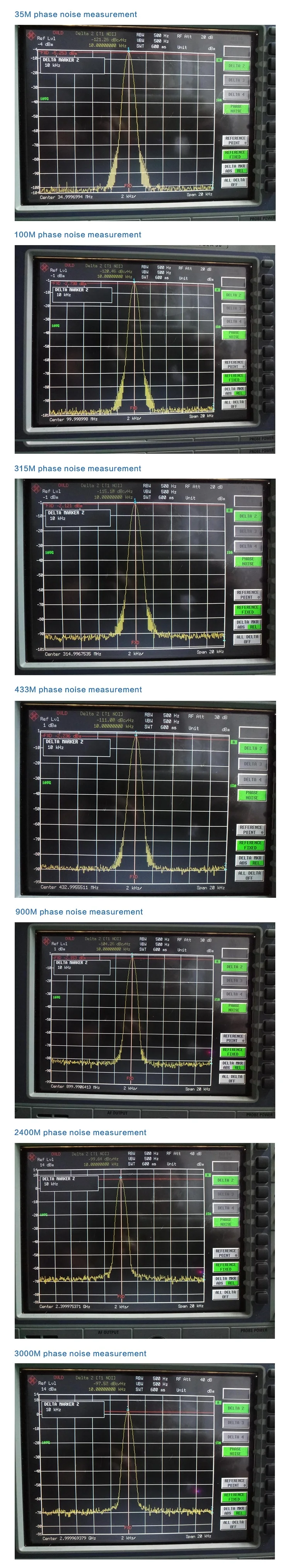
Phase noise: different frequency phase noise
Module output frequency range: 35MHz-4.4GHz
Frequency control step: 0.1MHz
Frequency sweep step time: 1mS(MIN)
Module output power: 7dBm (MAX); different frequency output power is different
Module output interface: SMA; 24-hour salt spray anti-oxidation
Module output signal: sine wave or square wave
Module output channel: 2 differential channels
Module output impedance: 50 ohm matching
Signal characteristics of the module: 35MHZ--2.2GHz square wave (fundamental frequency division) 2.2GHZ--4.4GHz sine wave (fundamental wave)
Module features: ultra-low phase noise, broadband RF PLL signal generator
Module application: RF signal frequency generator, sensor excitation source, line loss attenuation detection, scanning clock signal generator
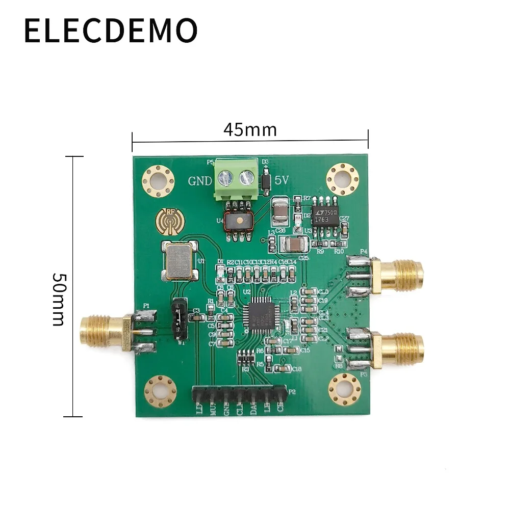
Module specification: 50*50*7mm length*width*height-PCB size
Module weight: 15g
Module working temperature: 0-75℃; civil grade
Module description
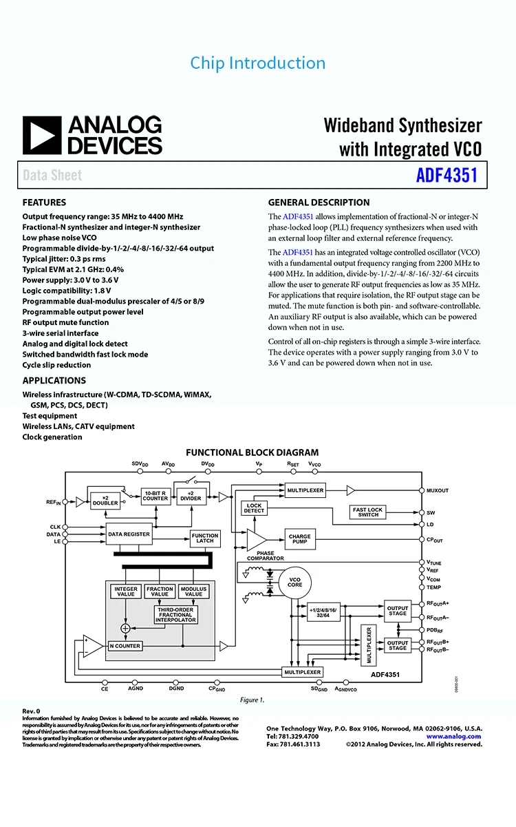
The ADF4351 is used in conjunction with an external loop filter and external reference frequency to implement an integer-N frequency-locked loop (PLL) frequency synthesizer.
The ADF4351 has an integrated voltage controlled oscillator (VCO) with a fundamental output frequency range of 2200 MHz to 4400 MHz. In addition, with 1/2/4/8/16/32/64 crossover circuits, users can generate RF output frequencies as low as 35 MHz. For applications requiring isolation, the RF output stage can be muted. The mute function can be controlled by pins or software. At the same time provide auxiliary RF output, and can be turned off when not in use.
Interface diagram
Dimensions
Precautions for using the module
(1) Since the module is a high-precision device, in order to avoid unnecessary interference, it is recommended to use a linear power supply.
(2) Correct power supply, reverse connection is prohibited, and the voltage should not exceed 5.5V.
(3) It is recommended to use a good patch cord to connect the instrument to observe the output signal. Poor contact or poor quality wires may cause signal attenuation or excessive noise.
(4) If you need to simply test the function of the module, it is recommended to use it with the control board of our store. Power is supplied to the PLL module first, and then the power is supplied to the control board to generate a waveform. Long press the middle button to switch the function.
(5) The distributed code is only used for the supporting main control board, and does not provide a single-chip microcomputer tutorial. Additional functions need to be developed by themselves.
(6) The phase noise, harmonics, power output and other corresponding indicators of the phase-locked loop module. The typical test parameters are included in the details.
Frequently asked questions
Q: Is the output waveform of AD4351 not a sine wave, and the harmonics are very large?
A: ADF4351 is a digital phase-locked loop. The frequency output below 2.2G is divided frequency output, the output waveform is similar to square wave, if you need a sine wave, you need an external filter.
Q: Can the fastest sweep speed of ADF4351 be only 1mS? Can the minimum step be only 0.1MHz?
A: The current loop bandwidth design and software design on the board, in order to support 35M-4.4G frequency can be output normally, so the minimum step and the fastest sweep time are fixed, and it is necessary to pursue smaller steps and faster sweep Time will require buyers to make hardware and software adjustments.
Q: What are the two lights on the board for the phase-locked loop module, but it doesn't light up after importing the program?
A: One is the power indication, the other is the lock indication, and both lights are on for normal operation. Generally, you need to power on the module first, and then power on the main control board. The power port on the main control board, the lock light is always on, and the module is normal output.