|
ADS1015 The ADS115 and ADS1015, 4-channel split version are ideal for adding high-resolution analog-to-digital conversion to any microprocessor-based project. These boards can run on power and logic signals between 2V and 5V, so they are compatible with all common 3.3V and 5V processors. Among them, 4 circuit boards can be controlled from the same 2-wire 12C bus, providing up to 16 single-ended or 8 differential channels. The programmable gain amplifier provides a gain of up to x16 for small signals. The two boards are very similar, but the resolution and speed are different. ADS1115 has a higher resolution, and ADS1015 has a higher sampling rate.
Product parameters:
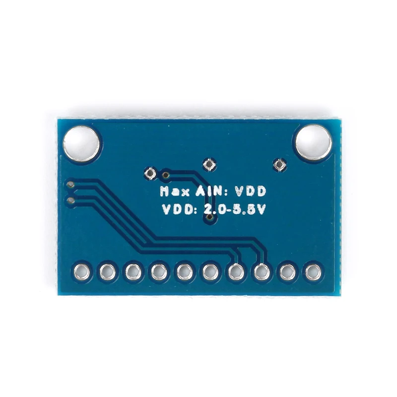
Power/logic level: 2.0V to 5.5V
Low current consumption: continuous mode: only 150μA single shot mode: automatic shutdown
Resolution: 12 bits
Programmable sampling rate: 128 to 3300 samples/sec
Internal low drift voltage reference
Internal oscillator
Internal: PGX16
12C interface: 4-pin optional address
Four single-ended or 2 differential inputs
Programmable comparator
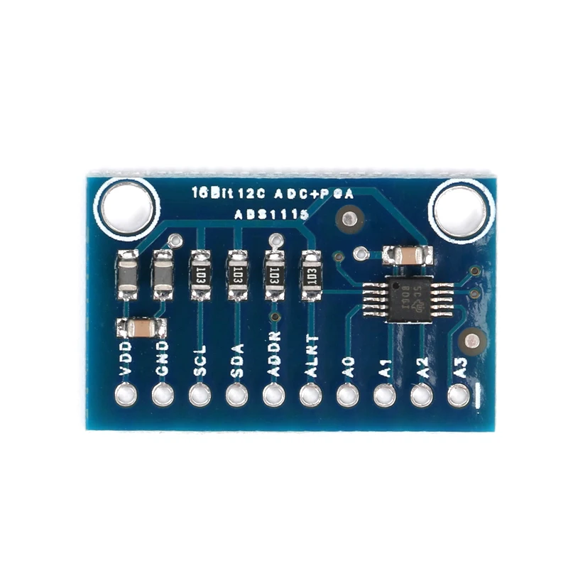
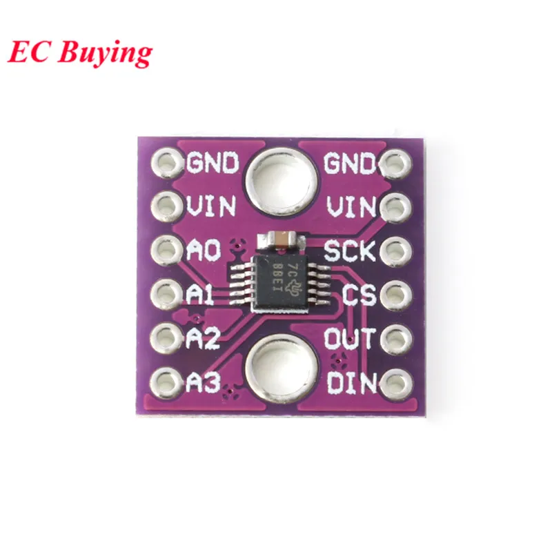
Pin description:
VDD: Positive power supply (3.3V/5V)
GND: ground, power negative
SCL: IIC clock line
SDA: llC data cable
ADDR: Determine the address of the lIC slave
ALRT: Digital comparator output or conversion ready
A0: differential channel 1, positive input or single-ended channel 1 input
A1: Differential channel 1, negative input or single-ended channel 2 input
A2: Differential channel 2, positive input or single-ended channel 3 input
A3: Differential channel 2, negative input or single-ended channel 4 input
Instructions for use:
The module IIC bus has a pull-up resistor, users do not need to pull it up, the default 7-bit IIC address of the module is 0x48 (1001000), and the chip uses a clever addressing method that allows one address pin (ADDR) to achieve four different the address of
When ADDR is grounded, the llC address is 0x48 (1001000)
When ADDR is connected to VDD, the IIC address is 0x49 (1001001)
When ADDR is connected to SDA, the IIC address is 0x4A (1001010)
When ADDR is connected to SCL, the IIC address is 0x4B (1001011)


GY-ADS1115 Features:
Application:
Package includes :
1 x GY-ADS1115
Gain Module
Note:if you need theGY-ADS1115(english) datasheet, please leave your e-mail, we will send to your e-mail. ADS1115 FEATURES DESCRIPTION:
23• ULTRA-SMALL QFN PACKAGE: The ADS1113, ADS1114, and ADS1115 are
2mm × 1,5mm × 0,4mm precision analog-to-digital converters (ADCs) with 16 • WIDE SUPPLY RANGE: 2.0V to 5.5V bits of resolution offered in an ultra-small, leadless • LOW CURRENT CONSUMPTION: QFN-10 package or an MSOP-10 package. The ADS1113/4/5 are designed with precision, power, and Continuous Mode: Only 150μA ease of implementation in mind. The ADS1113/4/5 Single-Shot Mode: Auto Shut-Down feature an onboard reference and oscillator. Data are • PROGRAMMABLE DATA RATE: transferred via an I2C-compatible serial interface; four 8SPS to 860SPS I2C slave addresses can be selected. The • INTERNAL LOW-DRIFT ADS1113/4/5 operate from a single power supply VOLTAGE REFERENCE ranging from 2.0V to 5.5V. • INTERNAL OSCILLATOR The ADS1113/4/5 can perform conversions at rates • INTERNAL PGA up to 860 samples per second (SPS). An onboard PGA is available on the ADS1114 and ADS1115 that • I2C™ INTERFACE: Pin-Selectable Addresses offers input ranges from the supply to as low as • FOUR SINGLE-ENDED OR TWO ±256mV, allowing both large and small signals to be DIFFERENTIAL INPUTS (ADS1115) measured with high resolution. The ADS1115 also features an input multiplexer (MUX) that provides two • PROGRAMMABLE COMPARATOR differential or four single-ended inputs. (ADS1114 and ADS1115) The ADS1113/4/5 operate either in continuous APPLICATIONS conversion mode or a single-shot mode that • PORTABLE INSTRUMENTATION automatically powers down after a conversion and greatly reduces current consumption during idle • CONSUMER GOODS periods. The ADS1113/4/5 are specified from –40°C • BATTERY MONITORING to +125°C 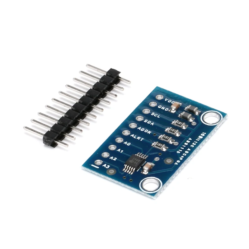
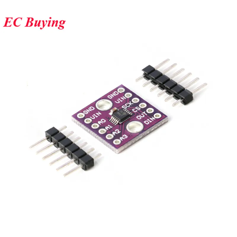
ADS1118
The ADS1118 is a precision, low power, 16-bit analog-to-digital converter (ADC) that provides all features necessary to measure the most common sensor signals in an ultra-small, leadless X2QFN-10 package or a VSSOP-10 package. The ADS1118 integrates a programmable gain amplifier (PGA), voltage reference, oscillator and high-accuracy temperature sensor. These features, along with a wide power supply range from 2 V to 5.5 V, make the ADS1118 ideally suited for power- and space-constrained, sensor-measurement applications.
The ADS1118 can perform conversions at data rates up to 860 samples per second (SPS). The PGA offers input ranges from ±256 mV to ±6.144 V, allowing both large and small signals to be measured with high resolution. An input multiplexer (MUX) allows to
measure two differential or four single-ended inputs.The high-accuracy temperature sensor can be used for system-level temperature monitoring or cold- junction compensation for thermocouples.
The ADS1118 operates either in continuous- conversion mode, or in a single-shot mode that automatically powers down after a conversion. Single-shot mode significantly reduces current consumption during idle periods. Data are transferred through a serial peripheral interface (SPI™). The ADS1118 is specified from –40°C to +125°C.
PCA9306
Features:
The IIC level shifter enables different signal levels of two IIC devices to communicate, and the 1.2V-3.3V reference level and the 1.8V-5.5V reference level are converted to each other. The low internal on-resistance allows for lower signal propagation delays. It is also possible to enable two different communication rate IIC devices to achieve normal communication, such as 400KHz on one side of the converter and 100KHz on the other side, but the maximum communication rate of the system is slightly less than 100KHz. Because of the small signal propagation delay, the device is mainly used for Works with SMBus devices and standard mode, fast mode and ultra fast mode Plus I2C bus devices. The maximum frequency depends on the RC time constant, but usually supports > 2 MHz.
The IIC level shifter cannot physically isolate the capacitor on either side of the bus. The bus capacitance on both sides should be limited to 400pF. If it is exceeded, the IIC bus buffer repeater should be connected. The PCA9306 can only isolate the two sides when the device is disabled and provides a voltage level shift upon activation. It is more advantageous than a discrete transistor voltage conversion solution because the switch is manufactured symmetrically, and the converter provides excellent ESD for low voltage devices. Protection while protecting lower ESD devices, the device's SCL and SDA are open-drain output devices.
Parameters:
Board VCC: 0V ~ 5.5V
Chip working reference voltage: Vref1, Vref2: 0V~5.5V
Working environment temperature: -40 ° C ~ 85 ° C
|


